Fpga configuration, Fpga programming over embedded usb-blaster, Fpga configuration –12 – Altera Arria V GX Starter Board User Manual
Page 20: Fpga programming over embedded usb-blaster –12
2–12
Chapter 2: Board Components
FPGA Configuration
Arria V GX Starter Board
November 2013
Altera Corporation
Reference Manual
lists the MAX V CPLD 5M2210 System Controller component reference and
manufacturing information.
FPGA Configuration
This section describes the FPGA, flash memory, and MAX V CPLD 5M2210 System
Controller device programming methods supported by the Arria V GX starter board.
The Arria V GX starter board supports the following three configuration methods:
■
Embedded USB-Blaster is the default method for configuring the FPGA at any
time using the Quartus II Programmer in JTAG mode with the supplied USB cable.
■
External USB-Blaster for configuring the FPGA using an external USB-Blaster that
connects to the JTAG programming header.
■
Flash memory download for configuring the FPGA using stored images from the
flash memory on either power-up or pressing the PGM_CONFIG push button (S1).
FPGA Programming over Embedded USB-Blaster
This configuration method implements a USB Type-B connector (J14), a USB 2.0 PHY
device (U23), and an Altera MAX II CPLD EPM570F100C5N (U21) to allow FPGA
configuration using a USB cable. This USB cable connects directly between the USB
port on the board and a USB port of a PC running the Quartus II software.
The embedded USB-Blaster in the MAX II CPLD EPM570F100C5N normally masters
the JTAG chain. To prevent contention between the JTAG masters, the embedded
USB-Blaster is automatically disabled when you connect an external USB-Blaster to
the JTAG chain through the JTAG connector.
T8
USB_CFG6
2.5-V
Reserved for future use
T9
USB_CFG7
2.5-V
Reserved for future use
R9
USB_CFG8
2.5-V
Reserved for future use
P9
USB_CFG9
2.5-V
Reserved for future use
M8
USB_CFG10
2.5-V
Reserved for future use
T10
USB_CFG11
2.5-V
Reserved for future use
H5
USB_CLK
2.5-V
On-board USB-Blaster II clock
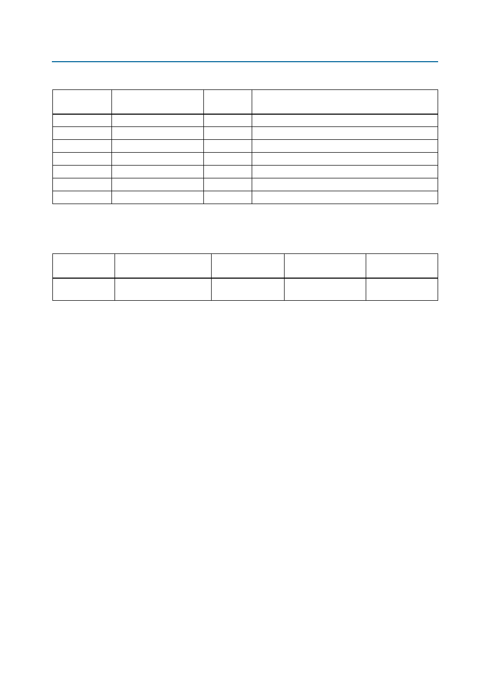
Table 2–5. MAX V CPLD 5M2210 System Controller Device Pin-Out (Part 6 of 6)
Board
Reference (U15)
Schematic Signal Name
I/O Standard
Description
Table 2–6. MAX II CPLD 5M2210 System Controller Component Reference and Manufacturing Information
Board Reference
Description
Manufacturer
Manufacturing
Part Number
Manufacturer
Website
U15
IC - MAX V CPLD 2210 LES,
256 FBGA 1.8 V VCCINT
Altera
Corporation
5M2210ZF256C4N