Altera Arria V GX Starter Board User Manual
Page 23

Chapter 2: Board Components
2–15
FPGA Configuration
November 2013
Altera Corporation
Arria V GX Starter Board
Reference Manual
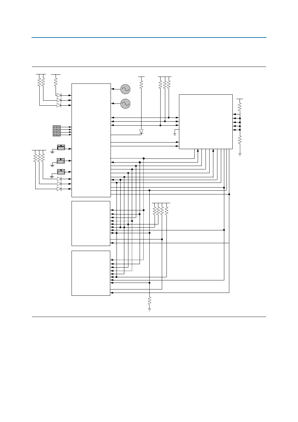
shows the PFL configuration.
f
For information about the flash memory map storage, refer to th
.
Figure 2–6. PFL Configuration
MAX V CPLD
5M2210 System Controller
Arria V FPGA
FPGA_DATA [7:0]
FPGA_DCLK
FLASH_A [26:1]
FLASH_D [31:0]
DATA [7:0]
DCLK
nSTATUS
nCONFIG
CONF_DONE
CONF_DONE
MSEL0
MSEL1
MSEL2
MSEL3
MSEL4
MSEL[4:0] also
connects to MAX V CPLD
Note:
At any one time, install either the
pull-up or pull-down resistor.
Refer to the datasheet for
valid MSEL settings to avoid
undesired FPGA behavior.
2.5 V
10 k
Ω
nCE
CFI Flash
FLASH_CEn0
FLASH_CEn1
FLASH_OEn
FLASH_WEn
FLASH_A [26:1]
FLASH_D [15:0]
FLASH_CEn0
FLASH_OEn
FLASH_WEn
FLASH_WPn
FLASH_ADVn
FPGA_nCONFIG
FPGA_CONF_DONE
FLASH_RYBSYn0
FLASH_RYBSYn0
FLASH_RYBSYn1
FPGA_nSTATUS
2.5 V
10 k
Ω
FLASH_ADVn
CONF_DONE_LED
2.5 V
FLASH_CLK
FLASH_CLK
FLASH_RSTn
FLASH_RESETn
FPP Mode
Flash Interface
56.2
Ω
100
Ω
56.2
Ω
56.2
Ω
50 MHz
100 MHz
2.5 V
2.5 V
2.5 V
ERROR
CONF_DONE
LOAD
CFI Flash
FLASH_A [26:1]
FLASH_D [31:16]
FLASH_CEn1
FLASH_OEn
FLASH_WEn
FLASH_WPn
FLASH_ADVn
FLASH_RYBSYn1
FLASH_CLK
FLASH_RESETn
Reserved
FACTORY_LOAD
CLK_ENABLE
CLK_SEL
MAX_RESETn
PGM_CONFIG
PGM_SEL
PGM_LED0
PGM_LED1
PGM_LED2
DIP Switch
10 k
Ω
2.5 V
DNI (0
Ω)
0
Ω
