Featured device: arria v gx fpga, I/o and transceiver resources, Featured device: arria v gx fpga –5 – Altera Arria V GX Starter Board User Manual
Page 13: I/o and transceiver resources –5

Chapter 2: Board Components
2–5
Featured Device: Arria V GX FPGA
November 2013
Altera Corporation
Arria V GX Starter Board
Reference Manual
Featured Device: Arria V GX FPGA
The Arria V GX starter board features a Arria V GX 5AGXFB3H4F35C4N device (U1)
in a 1152-pin FBGA package.
f
For more information about Arria V device family, refer to the
describes the features of the Arria V GX 5AGXFB3H4F35C4N device.
lists the Arria V GX component reference and manufacturing information.
I/O and Transceiver Resources
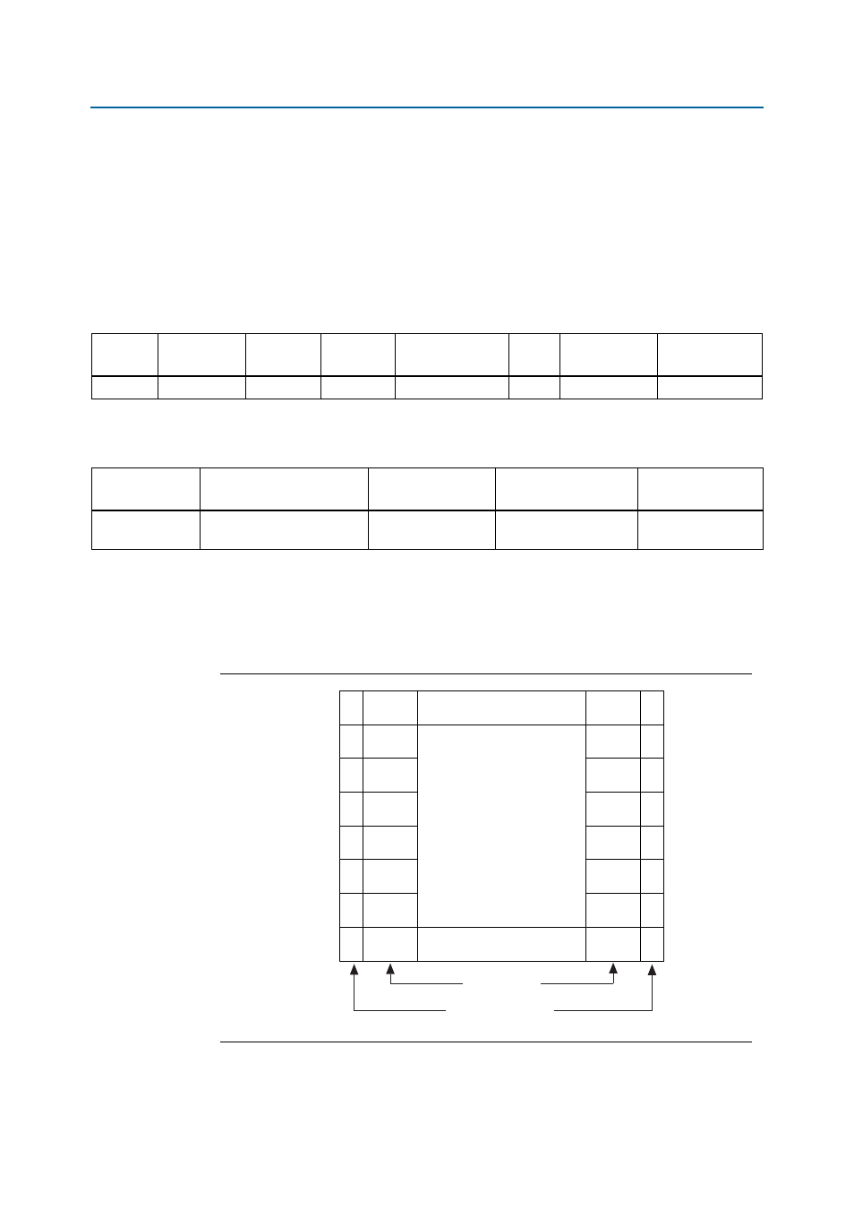
illustrates the bank organization and I/O count for the Arria V GX
5AGXFB3H4F35C4N device in the 1152-pin FBGA package.
Table 2–2. Arria V GX Features
ALMs
Equivalent
LEs
M10K RAM
Blocks
Total RAM
(Kbits)
18-bit × 19-bit
Multipliers
PLLs
Transceivers
Package Type
136,880
362,000
1,726
17,260
2,090
12
24
1152-pin FBGA
Table 2–3. Arria V GX Component Reference and Manufacturing Information
Board Reference
Description
Manufacturer
Manufacturing
Part Number
Manufacturer
Website
U1
FPGA, Arria V GX F1152,
362K LEs, leadfree
Altera
Corporation
5AGXFB3H4F35C4N
Figure 2–2. Arria V GX Device I/O Bank Diagram
Bank 3A
Total I/O in Each Bank
Bank Number
48
Bank 3B
32
Bank 3C
32
Bank 3D
32
Bank 4D
32
Bank 4C
32
Bank 8A
Bank 8B
Bank 8C
Bank 8D
Bank 7D
Bank 7C
48
32
32
32
32
32
Bank 4B
32
Bank 4A
32
Bank 7B
Bank 7A
32
31
Transceiver Block
Transceiver Block
5AGXFB3H4F35
