Additional information, Document revision history – Altera Stratix V GX FPGA Development Board User Manual
Page 73
October 2014
Altera Corporation
Stratix V GX FPGA Development Board
Reference Manual
Additional Information
This chapter provides additional information about the document and Altera.
Document Revision History
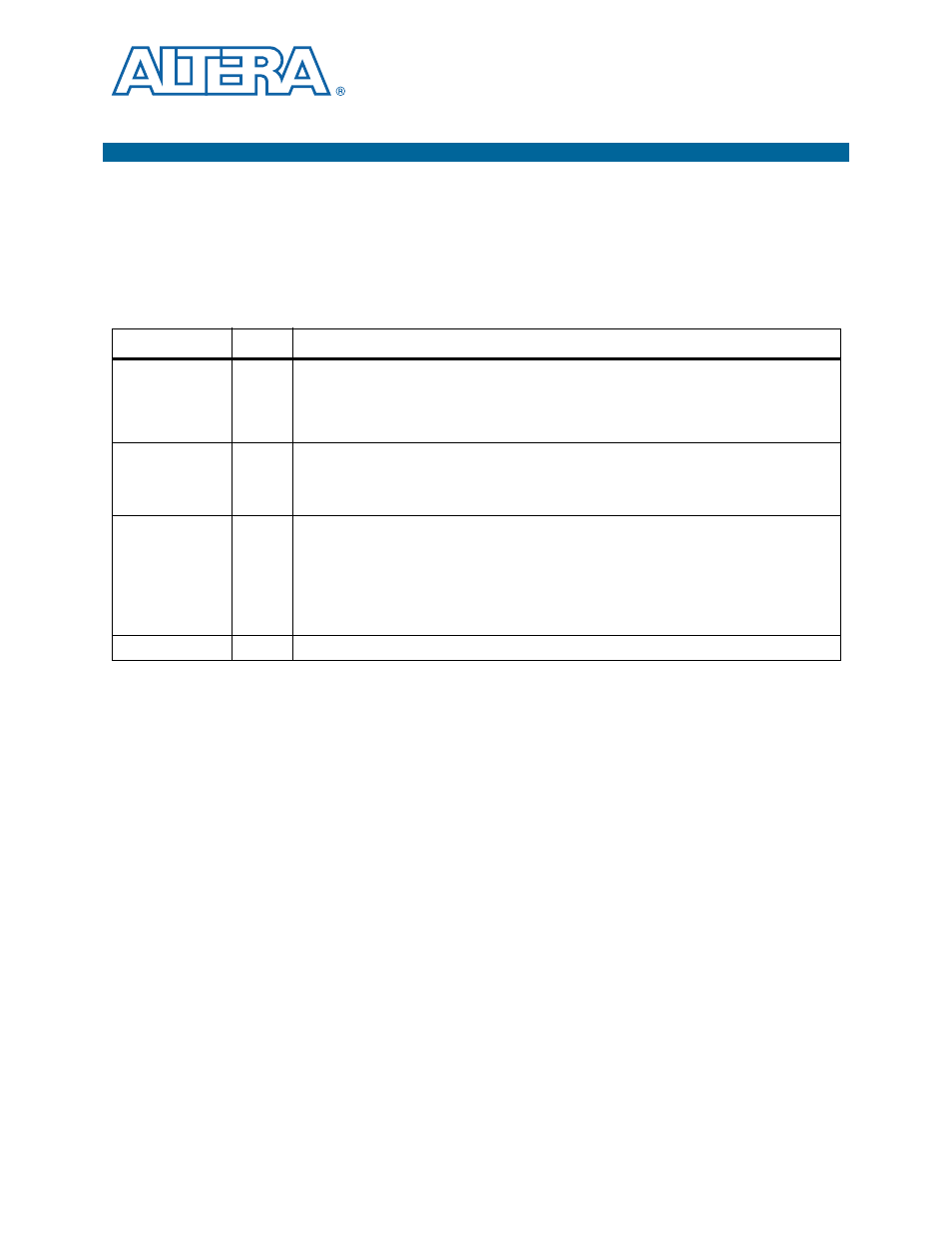
The following table shows the revision history for this document.
Date
Version
Changes
October 2014
1.5
■
Fixed typos in the Flash Pin Assignments, Schematic Signal Names, and Functions table
in Chapter 2.
■
Changed the standard I/O for the transmit bus (PCI Express Pin Assignments, Schematic
Signal Names, and Functions) to 1.5-V PCML from 1.4-V. Chapter 2.
April 2014
1.4
■
Corrected ALM amount in
section.
■
Updated Signal Types in
■
Corrected Power column title in
.
July 2012
1.3
■
Added RLDRAM II support for non-ES kits.
■
Revised the FPGA device pin numbers that connect to the on-board oscillator signals:
■
REFCLK2_QL1_P
: Changed from AB35 to AB34
■
REFCLK2_QL1_N
: Changed from AB34 to AB35
■
Converted document to new frame template and made textual and style changes.
March 2012
1.2
Updated the DDR3 interface frequency rate to 800 MHz.