Clock circuitry, On-board oscillators, Clock circuitry –23 – Altera Stratix V GX FPGA Development Board User Manual
Page 31: On-board oscillators –23
Chapter 2: Board Components
2–23
Clock Circuitry
October 2014
Altera Corporation
Stratix V GX FPGA Development Board
Reference Manual
Clock Circuitry
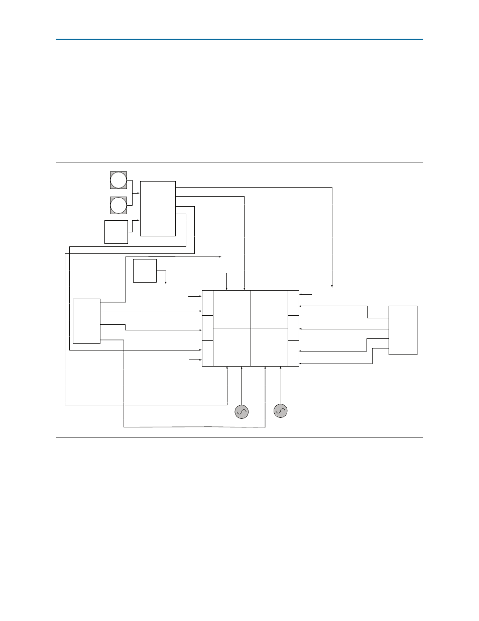
This section describes the board's clock inputs and outputs.
On-Board Oscillators
The development board includes a 50-MHz, 100-MHz, 125-MHz, and 156.25-MHz
programmable oscillators.
shows the default frequencies of all external
clocks going to the Stratix V GX FPGA development board.
Figure 2–5. Stratix V GX FPGA Development Board External Clock Inputs and Default Frequencies
SMA
REFCLK INPUT
SMA
Buffer
(100 MHz
Default)
Si570
(100 MHz
Default)
Si5388
156.25 MHz
625 MHz
270 MHz
100 MHz
REFCLK4_QR2_P/N
REFCLK5_QR2_P/N (HSMB)
REFCLK2_QR1_P/N (HSMB)
REFCLK1_QR0_P/N (HSMA)
REFCLK0_QR0_P/N (HSMA)
644.53125 MHz
282.5 MHz
125 MHz
125 MHz
125 MHz
100 MHz
100 MHz
100 MHz
100 MHz
CLK4
CLK0
CLK6
CLK22
CLK16
CLK9
REFCLK5_QL2_P/N (148.5 MHz)
SDI (148.5 M / 148.35 M)
REFCLK4_QL2_P/N (QSFP)
REFCLK2_QL1_P (QSFP)
REFCLK1_QL0_P/N
PCIE_REF_CLK_P/N
CLKINT
OP_P/N[1]
CLKINT
OP_P/N[0]
CLKIN_50
CLKINBO
T_P/N[0]
CLK_125_P/N
CLKINBO
T_P/N[1]
Si5388
CLK3
CLK2
CLK1
CLK0
Si571
148.5 MHz
Default
B8
QL2
QL1
QL0
B3
B4
B7
QR2
QR1
QR0
CLK3
CLK2
CLK1
CLK0
50 M
125 M