Jtag control dip switch, Jtag control dip switch –20 – Altera Stratix V GX FPGA Development Board User Manual
Page 28
2–20
Chapter 2: Board Components
Configuration, Status, and Setup Elements
Stratix V GX FPGA Development Board
October 2014
Altera Corporation
Reference Manual
lists the board settings DIP switch component reference and
manufacturing information.
JTAG Control DIP Switch
The JTAG control DIP switch (SW3) provides you an option to either remove or
include devices in the active JTAG chain. However, the Stratix V GX FPGA device is
always in the JTAG chain.
shows the switch controls and its descriptions.
lists the JTAG control DIP switch component references and
manufacturing information.
3
FACTORY_LOAD
ON : Load user 1 design from flash at power up.
OFF : Load factory design from flash at power up.
OFF
4
SECURITY_MODE
ON : Do not send FACTORY command at power-up.
OFF : Send FACTORY command at power-up.
ON
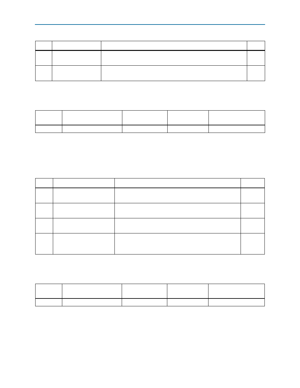
Table 2–12. Board Settings DIP Switch Controls (Part 2 of 2)
Switch Schematic Signal Name
Description
Default
Table 2–13. Board Settings DIP Switch Component Reference and Manufacturing Information
Board
Reference
Description
Manufacturer
Manufacturer
Part Number
Manufacturer Website
SW5
Four-Position slide DIP switch
C & K Components
TDA04H0SB1
Table 2–14. JTAG Control DIP Switch Controls
Switch
Schematic Signal Name
Description
Default
1
5M2210_JTAG_EN
ON : Bypass MAX V CPLD System Controller.
OFF : MAX V CPLD System Controller in-chain.
OFF
2
HSMA_JTAG_EN
ON : Bypass HSMC port A.
OFF : HSMC port A in-chain.
ON
3
HSMB_JTAG_EN
ON : Bypass HSMC port B.
OFF : HSMC port B in-chain.
ON
4
PCIE_JTAG_EN
ON : On-Board USB-Blaster II or external USB-Blaster is the chain
master.
OFF : PCI Express edge connector is the chain master.
ON
Table 2–15. JTAG Control DIP Switch Component Reference and Manufacturing Information
Board
Reference
Device Description
Manufacturer
Manufacturer
Part Number
Manufacturer Website
SW3
Four-Position slide DIP switch
C & K Components
TDA04H0SB1