Hsmc user-defined leds, Character lcd, Hsmc user-defined leds –29 – Altera Stratix V GX FPGA Development Board User Manual
Page 37: Character lcd –29
Chapter 2: Board Components
2–29
General User Input/Output
October 2014
Altera Corporation
Stratix V GX FPGA Development Board
Reference Manual
HSMC User-Defined LEDs
The HSMC port A and B have two LEDs located nearby. The LEDs are labeled TX and
RX. The LEDs display data flow to and from the connected HSMC cards. The LEDs
are driven by the Stratix V GX FPGA device. There are no board-specific functions for
the HSMC LEDs.
lists the HSMC user-defined LED schematic signal names and their
corresponding Stratix V GX FPGA pin numbers.
lists the HSMC user-defined LED component reference and the
manufacturing information.
Character LCD
The development board contains a single 14-pin 0.1" pitch dual-row header that
interfaces to a 16 character × 2 line Lumex LCD display. The LCD has a 14-pin
receptacle that mounts directly to the board's 14-pin header, so you can easily remove
it to access components under the display. You can also use the header for debugging
or other purposes.
summarizes the LCD pin assignments. The signal names and directions are
relative to the Stratix V GX FPGA.
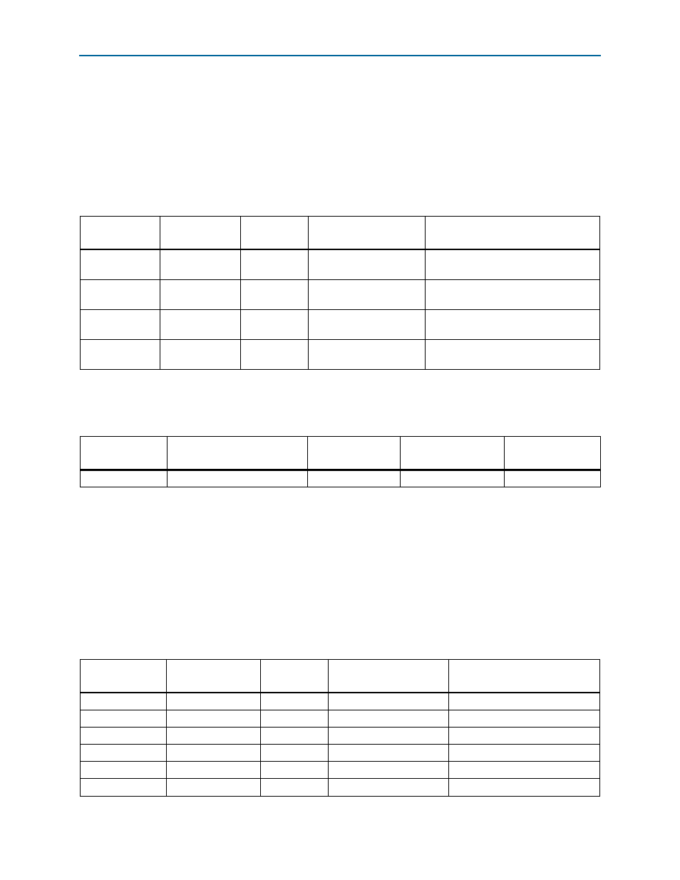
Table 2–32. HSMC User-Defined LED Schematic Signal Names and Functions
Board
Reference
Schematic
Signal Name
I/O Standard
Stratix V GX FPGA Device
Pin Number
Description
D3
HSMA_TX_LED
1.8-V
AU8
User-Defined LEDs.
Labeled TX for HSMC Port A.
D13
HSMA_RX_LED
1.8-V
AV8
User-Defined LEDs.
Labeled RX for HSMC Port A.
D11
HSMB_TX_LED
1.8-V
AP6
User-Defined LEDs.
Labeled TX for HSMC Port B.
D14
HSMB_RX_LED
1.8-V
AR6
User-Defined LEDs.
Labeled RX for HSMC Port B.
Table 2–33. HSMC User-Defined LED Component Reference and Manufacturing Information
Board Reference
Description
Manufacturer
Manufacturer
Part Number
Manufacturer
Website
D3, D11, D13, D14 Green LEDs, 0805, SMT, 2.0 V
Lumex Inc.
SML-LXT0805GW-TR
Table 2–34. LCD Pin Assignments, Schematic Signal Names, and Functions
Board Reference
(J15)
Schematic Signal
Name
I/O Standard
Stratix V GX FPGA Device
Pin Number
Description
4
LCD_D_Cn
2.5-V
AH10
LCD data or command select
5
LCD_WEn
2.5-V
AW10
LCD write enable
6
LCD_CSn
2.5-V
AU9
LCD chip select
7
LCD_DATA0
2.5-V
AP10
LCD data bus
8
LCD_DATA1
2.5-V
AN10
LCD data bus
9
LCD_DATA2
2.5-V
AM10
LCD data bus