Featured device: stratix v gx fpga, I/o resources, Featured device: stratix v gx fpga –5 – Altera Stratix V GX FPGA Development Board User Manual
Page 13: I/o resources –5
Chapter 2: Board Components
2–5
Featured Device: Stratix V GX FPGA
October 2014
Altera Corporation
Stratix V GX FPGA Development Board
Reference Manual
Featured Device: Stratix V GX FPGA
The Stratix V GX FPGA development board features the Stratix V GX FPGA
5SGXEA7K2F40C2N device (U15) in a 1517-pin FineLine BGA package.
f
For more information about the Stratix V device family, refer to
describes the features of the Stratix V GX FPGA 5SGXEA7K2F40C2N
device.
lists the Stratix V GX FPGA component reference and manufacturing
information.
I/O Resources
lists the Stratix V GX FPGA device pin count and usage by function on the
development board.
Power Supply
J18
PCI Express edge connector
Interfaces to a PCI Express root port such as an appropriate PC
motherboard.
J4
DC input jack
Accepts a 19-V DC power supply.
SW2
Power switch
Switch to power on or off the board when power is supplied from the
DC input jack.
Table 2–1. Stratix V GX FPGA Development Board Components (Part 4 of 4)
Board Reference
Type
Description
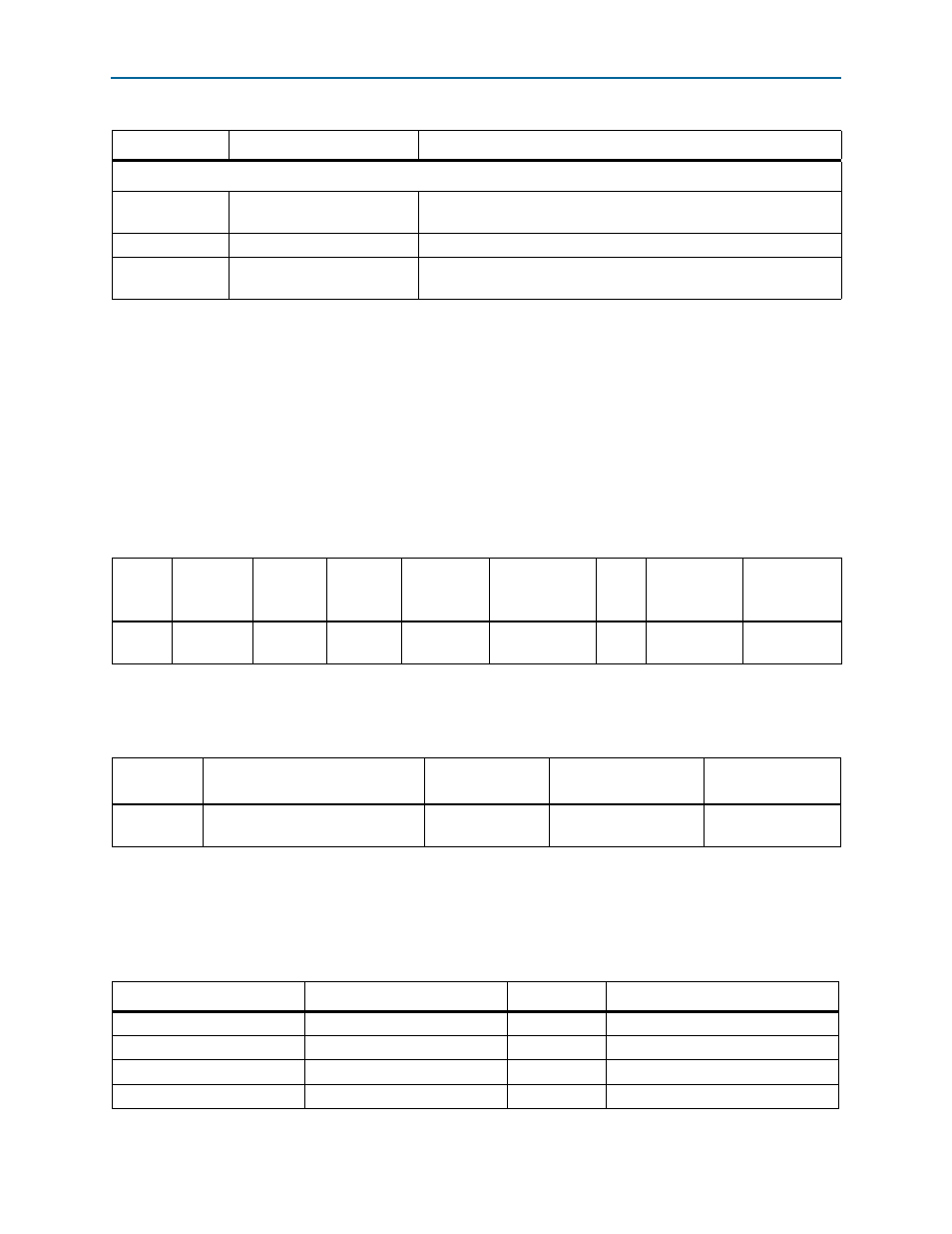
Table 2–2. Stratix V GX FPGA 5SGXEA7K2F40C2N Features
ALMs
Equivalent
LEs
Registers
M20K
Blocks
MLAB
Blocks (Mb)
18-bit × 18-bit
Multipliers
PLLs
Transceiver
Channels
(12.5 Gbps)
Package Type
234,720
622,000
939,000
2,560
7.16
512
28
36
1517-pin
FineLine BGA
Table 2–3. Stratix V GX FPGA Component Reference and Manufacturing Information
Board
Reference
Description
Manufacturer
Manufacturing
Part Number
Manufacturer
Website
U15
FPGA, Stratix V GX F1517, 622K
LEs, lead free
Altera
Corporation
5SGXEA7K2F40C2N
Table 2–4. Stratix V GX FPGA Pin Count and Usage (Part 1 of 2)
Function
I/O Standard
I/O Count
Special Pins
DDR3
1.5-V SSTL
126
1 Diff ×9DQS
RLDRAM II
1.8-V SSTL
57
1 Diff ×2 DQS
QDRII+ SRAM
1.8-V HSTL
67
1 Diff ×2 DQS
MAX V System Controller
1.5-V CMOS
8
—