Altera Stratix V GX FPGA Development Board User Manual
Page 18
2–10
Chapter 2: Board Components
MAX V CPLD System Controller
Stratix V GX FPGA Development Board
October 2014
Altera Corporation
Reference Manual
FPGA_CONFIG_D8
F3
AT32
2.5-V
FPGA configuration data
FPGA_CONFIG_D9
E1
AR31
2.5-V
FPGA configuration data
FPGA_CONFIG_D10
F4
AP31
2.5-V
FPGA configuration data
FPGA_CONFIG_D11
F2
AW34
2.5-V
FPGA configuration data
FPGA_CONFIG_D12
F1
AV34
2.5-V
FPGA configuration data
FPGA_CONFIG_D13
F6
AW31
2.5-V
FPGA configuration data
FPGA_CONFIG_D14
G2
AV31
2.5-V
FPGA configuration data
FPGA_CONFIG_D15
G3
AW32
2.5-V
FPGA configuration data
FPGA_CONFIG_D16
G1
AV32
2.5-V
FPGA configuration data
FPGA_CONFIG_D17
G4
AJ33
2.5-V
FPGA configuration data
FPGA_CONFIG_D18
H2
AH33
2.5-V
FPGA configuration data
FPGA_CONFIG_D19
G5
AL33
2.5-V
FPGA configuration data
FPGA_CONFIG_D20
H3
AK33
2.5-V
FPGA configuration data
FPGA_CONFIG_D21
J1
AK32
2.5-V
FPGA configuration data
FPGA_CONFIG_D22
J2
AJ32
2.5-V
FPGA configuration data
FPGA_CONFIG_D23
H5
AH31
2.5-V
FPGA configuration data
FPGA_CONFIG_D24
K2
AG31
2.5-V
FPGA configuration data
FPGA_CONFIG_D25
K5
AF31
2.5-V
FPGA configuration data
FPGA_CONFIG_D26
L1
AE31
2.5-V
FPGA configuration data
FPGA_CONFIG_D27
L2
AJ30
2.5-V
FPGA configuration data
FPGA_CONFIG_D28
K3
AH30
2.5-V
FPGA configuration data
FPGA_CONFIG_D29
M2
AR30
2.5-V
FPGA configuration data
FPGA_CONFIG_D30
L4
AP30
2.5-V
FPGA configuration data
FPGA_CONFIG_D31
L3
AU30
2.5-V
FPGA configuration data
FPGA_CVP_CONFDONE
N3
AT29
2.5-V
FPGA configuration via protocol done
FPGA_DCLK
J3
AC31
2.5-V
FPGA configuration clock
FPGA_nCONFIG
N1
AK35
2.5-V
FPGA configuration active
FPGA_nSTATUS
J4
AM5
2.5-V
FPGA configuration ready status
FPGA_PR_DONE
H1
AT30
2.5-V
FPGA partial reconfiguration done
FPGA_PR_ERROR
P2
AU29
2.5-V
FPGA partial reconfiguration error
FPGA_PR_READY
E2
AN29
2.5-V
FPGA partial reconfiguration ready
FPGA_PR_REQUEST
F5
AN30
2.5-V
FPGA partial reconfiguration request
HSMA_PRSNTn
B8
AW8
2.5-V
HSMC port A present
HSMB_PRSNTn
A8
AU7
2.5-V
HSMC port B present
M570_CLOCK
P11
—
1.8-V
25-MHz clock to on-board USB-Blaster for
sending FACTORY command
M570_PCIE_JTAG_EN
P12
—
1.8-V
A low signal disables the on-board
USB-Blaster when PCIe masters the JTAG
MAX5_BEN0
P10
U31
1.8-V
MAX V byte enable 0
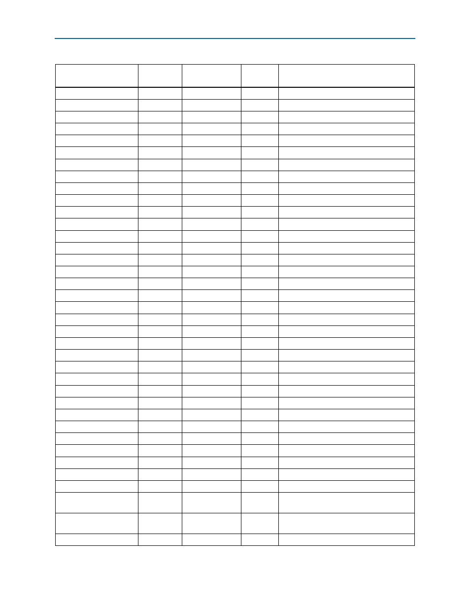
Table 2–5. MAX V CPLD System Controller Device Pin-Out (Part 4 of 6)
Schematic Signal Name
MAX V CPLD
Pin Number
Stratix V GX FPGA
Pin Number
I/O
Standard
Description