Altera Stratix V GX FPGA Development Board User Manual
Page 15
Chapter 2: Board Components
2–7
MAX V CPLD System Controller
October 2014
Altera Corporation
Stratix V GX FPGA Development Board
Reference Manual
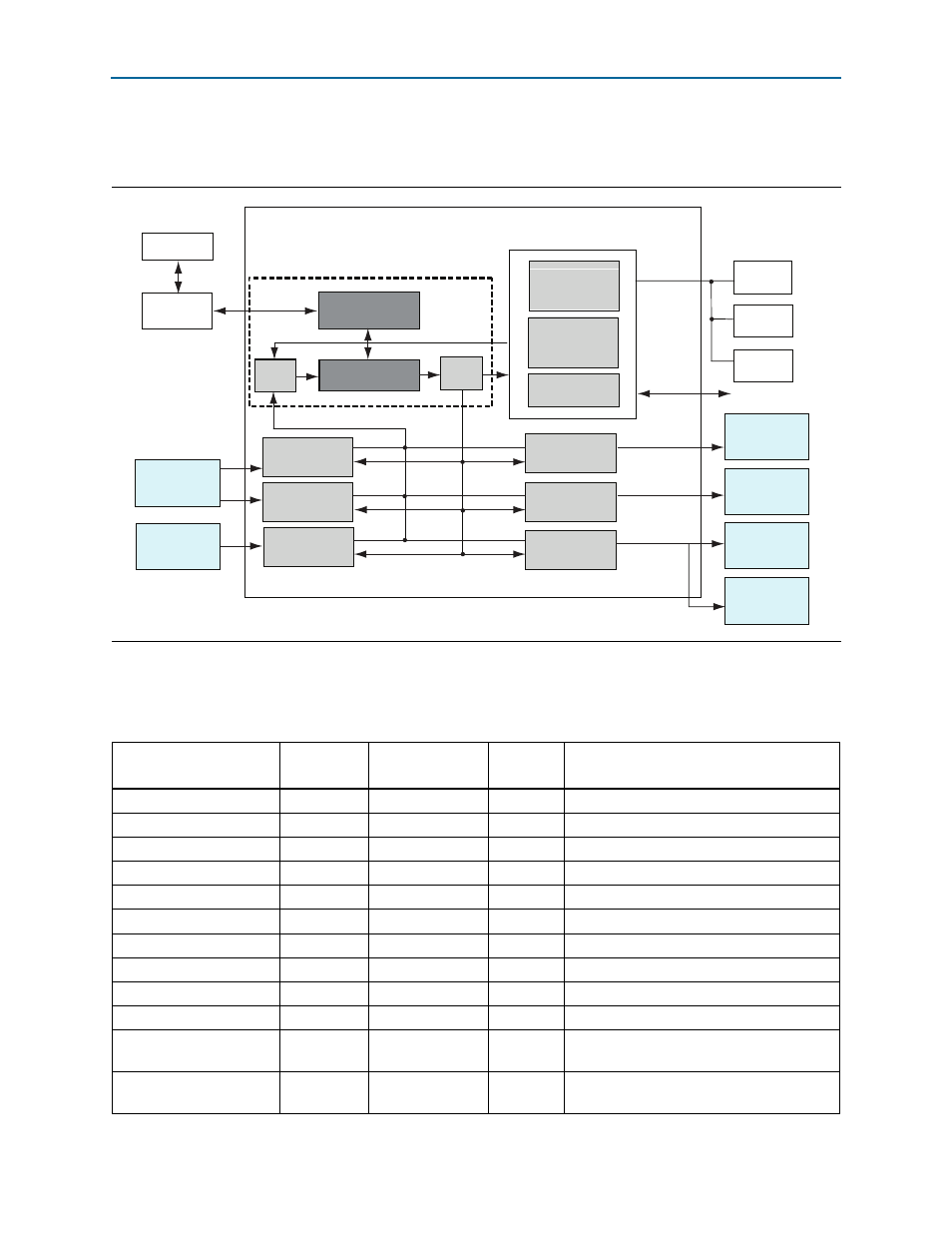
illustrates the MAX V CPLD System Controller's functionality and external
circuit connections as a block diagram.
lists the I/O signals present on the MAX V CPLD System Controller. The
signal names and functions are relative to the MAX V device (U4).
Figure 2–2. MAX V CPLD System Controller Block Diagram
Information
Register
On-Board
USB-Blaster II
Si571
Controller
Si5538
Controller
Si570
Controller
SLD-HUB
PFL
FSM BUS
MAX V System Controller
Power
Measurement
Results
Virtual-JTAG
PC
Temperature
Measurement
Results
FPGA
LTC2418
Controller
MAX1619
Controller
LTC2990
Controller
Flash
Decoder
Encoder
GPIO
JTAG Control
Flash
Control
Register
Si570
Programmable
Oscillator
Si571
Programmable
Oscillator
Si5338
Programmable
Oscillator
Si5338
Programmable
Oscillator
Table 2–5. MAX V CPLD System Controller Device Pin-Out (Part 1 of 6)
Schematic Signal Name
MAX V CPLD
Pin Number
Stratix V GX FPGA
Pin Number
I/O
Standard
Description
5M2210_JTAG_TMS
N4
—
2.5-V
MAX V JTAG TMS
CLK125_EN
B9
—
2.5-V
125 MHz oscillator enable
CLK50_EN
E9
—
2.5-V
50 MHz oscillator enable
CLK_CONFIG
J5
—
2.5-V
100 MHz configuration clock input
CLK_ENABLE
A15
—
2.5-V
DIP switch for clock oscillator enable
CLK_SEL
A13
—
2.5-V
DIP switch for clock select SMA or oscillator
CLKIN_50
J12
AN6
1.8-V
50 MHz clock input
CLOCK_SCL
C9
—
2.5-V
Programmable oscillator I
2
C clock
CLOCK_SDA
D9
—
2.5-V
Programmable oscillator I
2
C data
CPU_RESETn
D10
AM34
2.5-V
FPGA reset push button
FACTORY_LOAD
A2
—
2.5-V
DIP - load factory image or user1 image from
flash at power-up
FACTORY_REQUEST
R14
—
1.8-V
On-Board USB-Blaster II request to send
FACTORY command