Altera Stratix V GX FPGA Development Board User Manual
Page 38
2–30
Chapter 2: Board Components
General User Input/Output
Stratix V GX FPGA Development Board
October 2014
Altera Corporation
Reference Manual
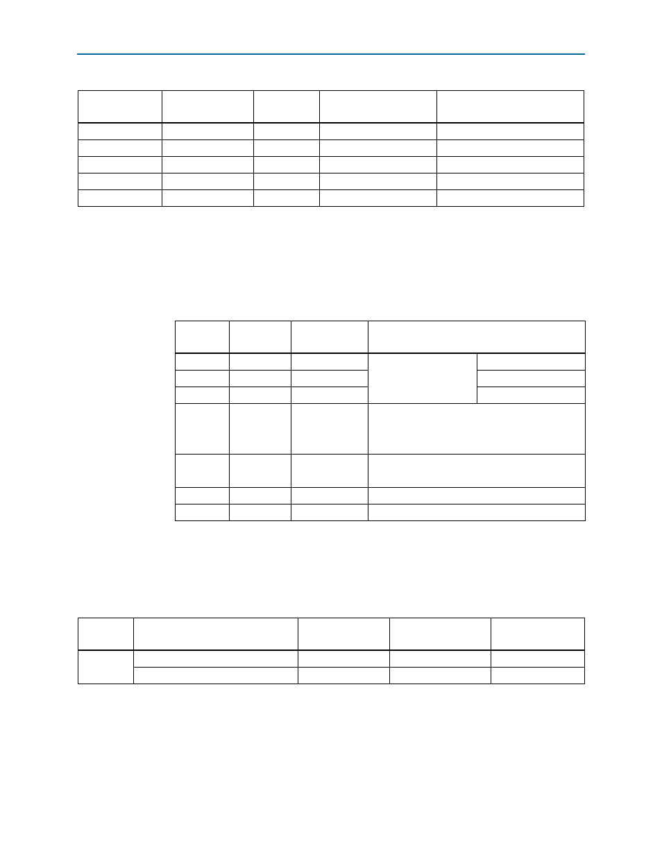
shows the LCD pin definitions, and is an excerpt from the Lumex data
sheet.
f
For more information such as timing, character maps, interface guidelines, and other
related documentation, visi
1
The particular model used does not have a backlight and the LCD drive pin is
connected to 5 V for maximum pixel drive.
lists the LCD component references and the manufacturing information.
10
LCD_DATA3
2.5-V
AL10
LCD data bus
11
LCD_DATA4
2.5-V
AP9
LCD data bus
12
LCD_DATA5
2.5-V
AN9
LCD data bus
13
LCD_DATA6
2.5-V
AT9
LCD data bus
14
LCD_DATA7
2.5-V
AR9
LCD data bus
Table 2–34. LCD Pin Assignments, Schematic Signal Names, and Functions
Board Reference
(J15)
Schematic Signal
Name
I/O Standard
Stratix V GX FPGA Device
Pin Number
Description
Table 2–35. LCD Pin Definitions and Functions
Pin
Number
Symbol
Level
Function
1
V
DD
—
Power supply
5 V
2
V
SS
—
GND (0 V)
3
V
0
—
For LCD drive
4
RS
H/L
Register select signal
H: Data input
L: Instruction input
5
R/W
H/L
H: Data read (module to MPU)
L: Data write (MPU to module)
6
E
H, H to L
Enable
7–14
DB0–DB7
H/L
Data bus, software selectable 4-bit or 8-bit mode
Table 2–36. LCD Component References and Manufacturing Information
Board
Reference
Description
Manufacturer
Manufacturer
Part Number
Manufacturer
Website
J15
2×7 pin, 100 mil, vertical header
Samtec
SSW-107-01-G-D
2×16 character display, 5×8 dot matrix Lumex Inc.
LCM-S01602DSR/C