Memory, Ddr3, Memory –46 – Altera Stratix V GX FPGA Development Board User Manual
Page 54: Ddr3 –46
2–46
Chapter 2: Board Components
Memory
Stratix V GX FPGA Development Board
October 2014
Altera Corporation
Reference Manual
lists the QSFP interface component reference and manufacturing
information.
Memory
This section describes the board’s memory interface support, signal names, types, and
connectivity relative to the Stratix V GX FPGA device. The board has the following
memory interfaces:
■
DDR3
■
QDRII+
■
RLDRAM II
■
Flash
f
For more information about the memory interfaces, refer
page of the Altera website.
DDR3
The development board supports a 16Mx72x8 bank DDR3 SDRAM interface for very
high-speed sequential memory access. The 72-bit data bus comprises of four x16
devices and one x8 device with a single address or command bus. This interface
connects to the vertical I/O banks on the top edge of the FPGA.
The DDR3 devices shipped with this board are running at 800 MHz, for a total
theoretical bandwidth of over 115.2 Gbps. These devices run at a minimum frequency
of 303 MHz.
11
QSFP_SCL
3.3-V LVTTL
AD30
QSFP serial 2-wire clock
12
QSFP_SDA
3.3-V LVTTL
AC30
QSFP serial 2-wire data
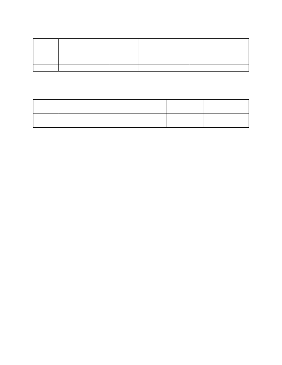
Table 2–48. 40G QSFP Pin Assignments, Schematic Signal Names, and Functions (Part 2 of 2)
Board
Reference
(J12)
Schematic
Signal Name
I/O Standard
Stratix V GX FPGA Device
Pin Number
Description
Table 2–49. QSFP Interface Component Reference and Manufacturing Information
Board
Reference
Description
Manufacturer
Manufacturing
Part Number
Manufacturer
Website
J12
QSFP cage
Tyco Electronics
1888617-1
QSFP connector
Tyco Electronics
1761987-9