Figure 3-5: configuration write to function 0 – Altera Arria V GZ Avalon-ST User Manual
Page 33
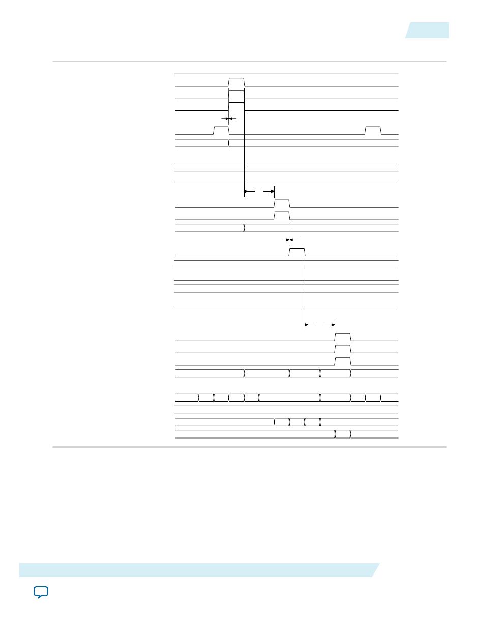
Figure 3-5: Configuration Write to Function 0
RxStMask_o
RxStSop_i
RxStEop_i
RxStValid_i
RxStReady_o
RxStData_i[255:0
cfg_addr_o[31:0]
cfg_rden_o
cfg_wren_
cfg_writeresponserequest
_
cfg_wrdata_o[31:0]
cfg_writeresponsevalid
cfg_writeresponse_i[2:0]
cfg_waitrequest
_
cfg_be_o[3:0]
TxStReady_i
TxStSop_o
TxStEop_o
TxStValid_o
TxStData_o[255:0]
rx_state[10:0]
rxavl_state[3:0]
rxcfg_state[4:0]
tx_state[1:0]
000000000000 . 0000000
00000060
01000004
. 0000000
..800040A000001
00000000000000000000000601000004000000F4408001
00000F4408001
.
000 003 005 021
009
081
000 003
03
09
11
3
0
1
2
3
Timing for Memory Write and Read of Function 1 256-Bit Avalon-ST Interface
The following timing diagram illustrates memory to Function 1 which occurs in the simulation starting at
time 99102 ns.
UG-01127_avst
2014.08.18
Timing for Memory Write and Read of Function 1 256-Bit Avalon-ST Interface
3-9
Getting Started with the Configuration Space Bypass Mode Qsys Example Design
Altera Corporation