Systolic delay register, Systolic delay register -6, Figure 6-6: pre-adder constant mode – Altera Integer Arithmetic IP User Manual
Page 59: Whereas the
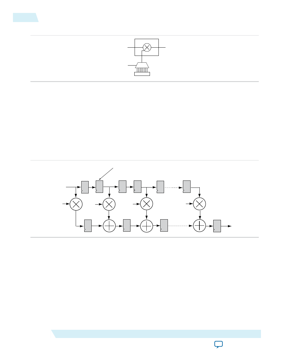
Figure 6-6: Pre-adder Constant Mode
a0
Mult0
result
coef
coefsel0
Systolic Delay Register
In a systolic architecture, the input data is fed into a cascade of registers acting as a data buffer. Each
register delivers an input sample to a multiplier where it is multiplied by the respective coefficient. The
chain adder stores the gradually combined results from the multiplier and the previously registered result
from the
chainin[]
input port to form the final result. Each multiply-add element must be delayed by a
single cycle so that the results synchronize appropriately when added together. Each successive delay is
used to address both the coefficient memory and the data buffer of their respective multiply-add elements.
For example, a single delay for the second multiply add element, two delays for the third multiply-add
element, and so on.
Figure 6-7: Systolic Registers
x(t)
c(0)
c(1)
c(2)
y(t)
c(N-1)
Systolic registers
S
-1
S
-1
S
-1
S
-1
S
-1
S
-1
S
-1
S
-1
S
-1
S
-1
x(t) represents the results from a continuous stream of input samples and y(t) represents the summation
of a set of input samples, and in time, multiplied by their respective coefficients. Both the input and
output results flow from left to right. The c(0) to c(N-1) denotes the coefficients. The systolic delay
registers are denoted by S
-1
, whereas the
–1
represents a single clock delay. Systolic delay registers are
added at the inputs and outputs for pipelining in a way that ensures the results from the multiplier
operand and the accumulated sums stay in synch. This processing element is replicated to form a circuit
that computes the filtering function. This function is expressed in the following equation.
6-6
Systolic Delay Register
UG-01063
2014.12.19
Altera Corporation
ALTERA_MULT_ADD (Multiply-Adder)