Design example 1: calculation of parity bits, Design example 2: altecc_decoder, Understanding the simulation results – Altera Integer Arithmetic IP User Manual
Page 50: Design example 2: altecc_decoder -12, Understanding the simulation results -12
• The encoded input data for F0 is 14F0 (1 0100 1111 0000 in binary), as seen on the output port, q[], at
17.5 ns.
Design Example 1: Calculation of Parity Bits
Design Example 2: ALTECC_DECODER
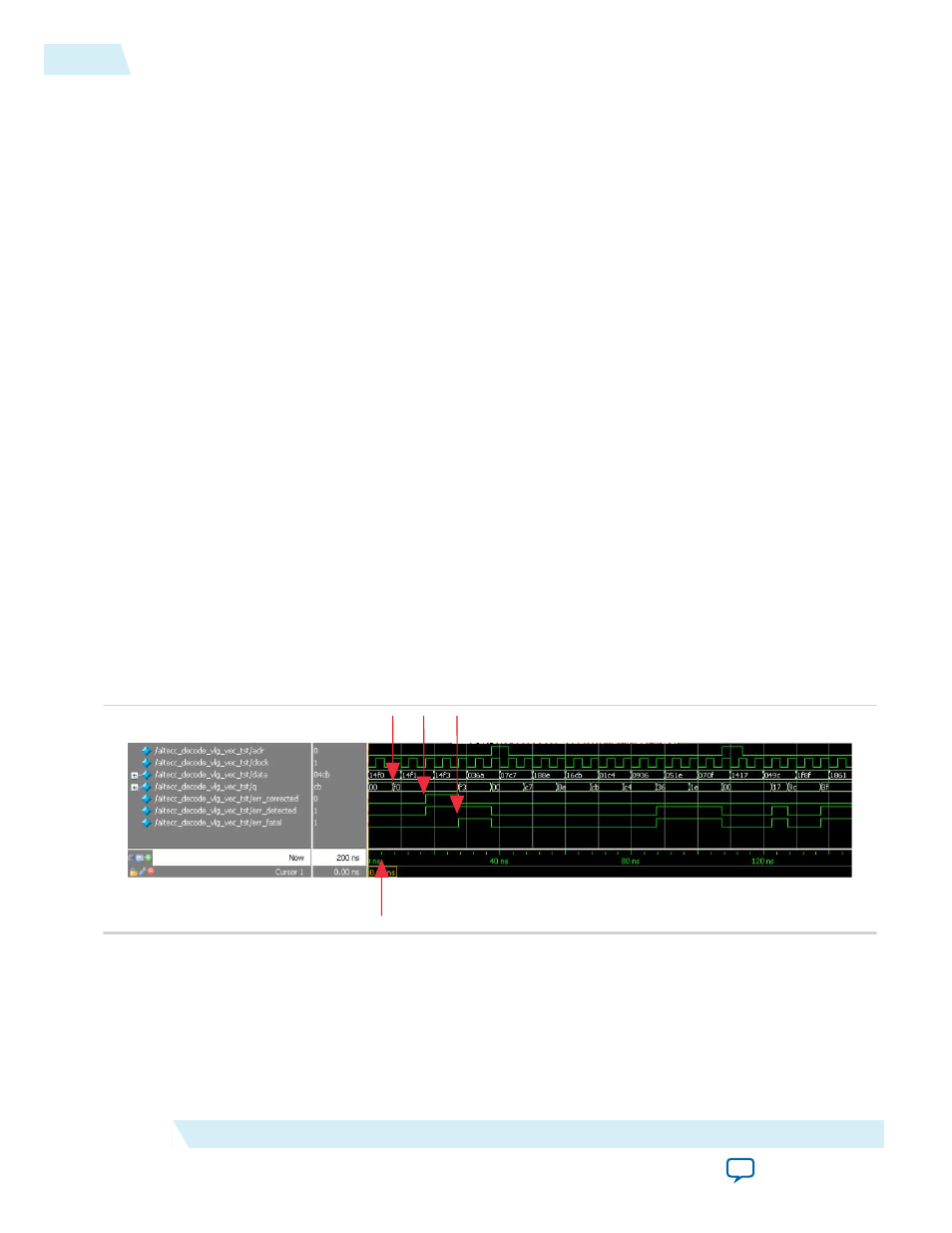
This design example uses the ECC decoder to decode input code words of 13-bit widths to generate 8 bits
of output data. An asynchronous clear signal is also used to illustrate how the signal affects the registered
ports. This example uses the MegaWizard Plug-In Manager in the Quartus II software.
• altecc_decode.qar (archived Quartus II design files)
• altecc_decode_ex_msim (ModelSim-Altera files)
Understanding the Simulation Results
The following settings are observed in this example:
• The
data[]
input width is set to 13 bits
• The output port,
q[]
has a width of 8 bits
• The asynchronous clear (
aclr
) signal is enabled
• Pipelining is enabled, with an output latency of 2 clock cycles. Hence, the result is seen on the
q[]
port
two clock cycles after the input data is available
The following figure shows the expected simulation results in the ModelSim-Altera software.
Figure 5-6: Design Example 2: Simulation Waveform for the ECC Decoder
The following sequence corresponds with the numbered items in the figure.
1. The decoder decodes the code word 14F0 at the first rising edge of the clock at 2.5 ns. In this case, the
input code word is not corrupted. The 13-bit input code word 14F0 (1 0100 1111 0000 in binary) is
decoded to generate an 8-bit output data of F0. The following table lists the arrangement of parity bits
and data bits in the code word 14F0. The prefixes P and D denote parity and data respectively.
5-12
Design Example 1: Calculation of Parity Bits
UG-01063
2014.12.19
Altera Corporation
ALTECC (Error Correction Code: Encoder/Decoder)