Jtag configuration setup, Jtag configuration setup -3 – Altera MAX 10 FPGA User Manual
Page 33
•
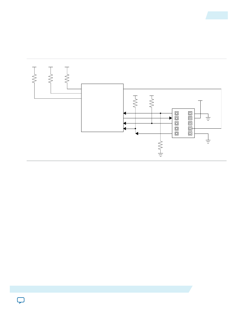
JTAG Configuration Setup
To configure MAX 10 device using a download cable, connect the device as shown in the following figure.
Figure 3-1: JTAG Configuration of a Single Device Using a Download Cable
V
CCIO
10 kΩ
V
CCIO
10 kΩ
V
CCIO
10 kΩ
nSTATUS
CONF_DONE
nCONFIG
MAX 10
JTAGEN
TCK
TDO
TMS
TDI
2
4
6
8
10
1
3
5
7
9
V
CCIO
10 kΩ
V
CCIO
10 kΩ
V
CCIO
JTAGEN
1 kΩ
Download Cable
(JTAG Mode)
10-Pin Male Header
To configure a device in a JTAG chain, the programming software sets the other devices to bypass mode.
A device in bypass mode transfers the programming data from the
TDI
pin to the
TDO
pin through a single
bypass register. The configuration data is available on the
TDO
pin one clock cycle later.
The Quartus II software uses the
CONF_DONE
pin to verify the completion of the configuration process
through the JTAG port:
•
CONF_DONE
pin is low—indicates that the configuration has failed.
•
CONF_DONE
pin is high—indicates that the configuration was successful.
After the configuration data is transmitted serially using the JTAG
TDI
port, the
TCK
port is clocked to
perform device initialization.
Voltage Overshoot Prevention
To prevent voltage overshoot, power up the download cable to 2.5 V when VCCIO of the JTAG pins are
2.5 V to 3.3 V. Tie the
TCK
pin to ground. If the VCCIO of the JTAG pins are using 1.5 V or 1.8 V, the
download cable should be powered by the same VCCIO. For single-supply device which has to power-up
the download cable within the range of 3.0 V to 3.3 V, Altera recommends you to add external resistor or
diode.
UG-M10CONFIG
2015.05.04
JTAG Configuration Setup
3-3
MAX 10 FPGA Configuration Design Guidelines
Altera Corporation