Elecraft K1 User Manual
Page 19

18
E
LECRAFT
Top of
board
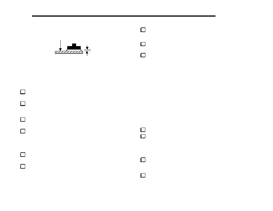
1/16”
Figure 5-3
Figure 5-3 shows a side view of a switch that is properly mounted
(spacing tool not shown). The leads of the switches will just be
visible on the bottom of the board. Proper switch height is
important for maintaining an even appearance.
Once S1 is seated correctly, solder the leads on the bottom side
of the board. Leave the spacing tool in place while soldering.
Install S3, once again using the switch spacing tool to adjust
the switch height. When soldering S3, be careful not to contact the
plastic body of J1 with the soldering iron.
Install switches S2, S4, S5, and S6 using the same technique.
Note: Switch caps will be installed later.
Install these parts on the top side of the board. Solder them on
the bottom side, using a minimum of solder.
__ R8, 22 (RED-RED-BLK)
__ C4, .047 µF (473)
Trim the leads of R8 and C4 as close to the board as possible
so that they won't interfere with the 40-pin IC socket (next step).
Install the 40-pin IC socket at U1, on the bottom side of the
board. The board is labeled "SOCKET" at this location. Orient the
socket's notched end to the left (the pin 1 end). To hold the socket
in place, bend pins 1 and 21 outward slightly; these two pins are
diagonally opposite. Solder only these two pins.
If the socket does not appear to be seated flat on the PC
board, reheat these two pins while pressing on the socket. If the
leads of C4 hit the socket, trim them closer to the board.
Solder the remaining pins of U1. (U1 itself will be installed in
the socket in a later step.)
Install and solder the following components. When soldering
components near the push-button switches, be careful not to touch
the switches with the soldering iron.
Top side:
__ R4 and __ R5, 10 k (BRN-BLK-ORG)
__ R11, 100 k (BRN-BLK-YEL)
Bottom side:
__ R6, 12.7 k, 1% (BRN-RED-VIO-RED)
__ R7, 3.92 k, 1% (ORG-WHT-RED-BRN)
__ R9, __ R10, and __ R19, 100 k (BRN-BLK-YEL)
__ R13, 470 (YEL-VIO-BRN)
__ R12, 2.7 k (RED-VIO-RED)
__ R14 and __ R15, 1 k (BRN-BLK-RED)
__ R16, 2.7 k (RED-VIO-RED)
__ C5 and __ C6, .01 µF (103)
Install capacitors C1 and C2 (82 pF), near U1.
Locate resistor network RP1. ("RP" means "resistor pack,"
another name for resistor networks.) One end of RP1 has a
band or dot,
indicating pin 1. RP1 should be labeled 77083102, 83C102, or
8A3102G. If the labeling differs, verify the resistance. You should
measure about 1.0 k between each pair of adjacent pins.
Install RP1 on the bottom side of the board. The end with a
dot or bar should be oriented towards pin 1 of the PCB outline.
When soldering RP1, keep the iron tip away from S4 and S5.
Install and solder the two 82-µH RF chokes, RFC1 and RFC2
(GRAY-RED-BLK).
