Figure 8.13. footprint dimensions – Atec Agilent-346a User Manual
Page 52
52
Designing and Probing with Target Connections
Agilent Logic Analyzers with 90-pin Pod Connectors
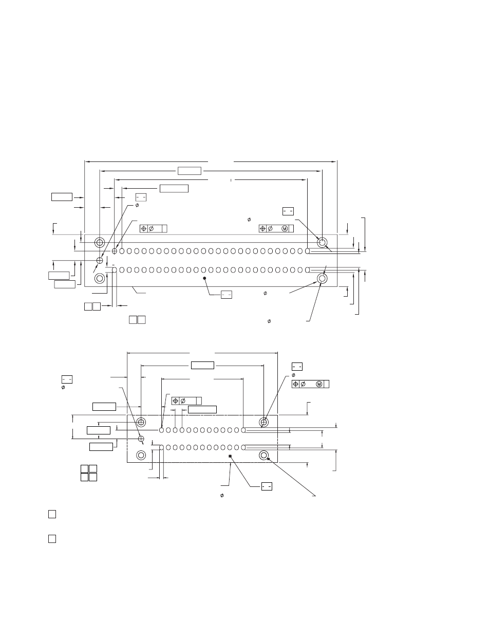
Probe Footprint Dimensions
Use these probe footprint
dimensions for the PC board pads
and holes for attaching the reten-
tion module.
Figure 8.13. Footprint dimensions
34.04 mm
26.00 mm
29.97 mm
2.53 mm
6.99 mm
3.25 mm
1.35 mm
retention hole pads
both sides
1.83 mm
1.00 mm typ
2.03 mm
3.49 mm
1.27 mm
2.41 mm
pad height 54x
1
2
1
B
B27
A27
.15 B
.15 B
R 0.29 mm
2
0.58 mm
pad width 54x
footprint keep
out boundary
0.81
±
0.03 mm
(keying/alignment hole)
A1
B1
0.71 mm
A
C
1.99 mm
0.79
±
0.08 mm pth
0.79
±
0.08 mm
pth 4x
22.05 mm
12.00 mm
6.99 mm
1.83 mm
2.54 mm
3.25 mm
3.49 mm
2.03 mm
footprint keep out boundary
17.98 mm
2.99 mm
2.41 mm
1.27 mm
1.00 mm typ
B
0.81 mm +
_ 0.03 npth
(keying/alignment hole)
.152 B
R 0.29 mm 4x
.127 B
C
0.79 mm +
_ 0.08 pth 4x
1
2
0.71 mm pad height 26x
1
2
0.58 mm pad width 26x
1.35 mm retention hole pads (both sides)
A
1.
2.
3.
4.
5.
6.
Must maintain a solder mask web between pads when traces are
routed between the pads on the same layer. Soldermask may not
encroach onto the pads within the pad dimension shown.
Via in pad not allowed on these pads. Via edges may be tangent
to pad edges as long as a solder mask web between vias and pads
is maintained.
Permissible surface finishes on pads are HASL, immersion silver,
or gold over nickel.
Footprint is compatible with retention module,
Agilent part # E5387-68702.
Retention module dimensions are 34.04 mm x 7.01 mm x 4.98 mm
tall relative to the top surface of the PDB. Retention pins extend
4.32 mm beyond the bottom surface of the RM through the PCB.
Assume normal artwork tolerances for pad size dimensions.
Soft touch
Half-size soft touch