Atec Agilent-346a User Manual
Page 21
21
Designing and Probing with Target Connections
For All Agilent Logic Analyzers with 40-pin Pod Connectors
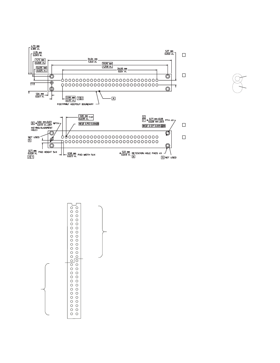
Figure 5.9. Pro Series soft touch footprint dimensions (see drawing notes).
Drawing notes:
Maintain a solder mask web between pads when
traces are routed between the pads on the same
layer. The solder mask may not encroach onto the
pads within the pad dimension shown.
VIAs not allowed on these pads.
VIA edges may be tangent to pad
edges as long as a solder mask
web between VIAs and pads is
maintained.
Surface finishes on pads should be HASL
immersion silver, or gold over nickel.
This footprint is compatible with retention module
Agilent part number E5405-68702.
This through hole is not used with the Agilent
retention module.
Plated through hole should not be tied to ground
plane for thermal relief.
A1
A2
A3
A4
A5
A6
A7
A8
A9
A10
A11
A12
A13
A14
A15
A16
A17
A18
A19
A20
A21
A22
A23
A24
A25
A26
A27
D0
D1
GND
D4
D5
GND
CK 1+
GND/NC
GND
D10
D11
GND
D14
D15
GND
D2
D3
GND
D6
D7
GND
D8
D9
GND
D12
D13
GND
GND
D2
D3
GND
D6
D7
GND
D8
D9
GND
D12
D13
GND
D0
D1
GND
D4
D5
GND
GND/NC
CK 2+
GND
D10
D11
GND
D14
D15
B1
B2
B3
B4
B5
B6
B7
B8
B9
B10
B11
B12
B13
B14
B15
B16
B17
B18
B19
B20
B21
B22
B23
B24
B25
B26
B27
Logic
analyzer
odd pod
Logic
analyzer
even pod
Figure 5.10. Pad numbers for E5404/06A 34-channel
single-ended probes.
1
VIA
Pad
2
3
4
5
6