Rainbow Electronics DS2153Q User Manual
Page 9
DS2153Q
022697 9/48
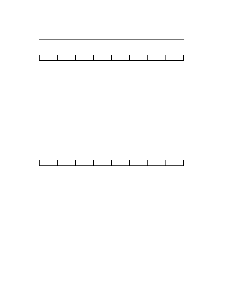
RCR2: RECEIVE CONTROL REGISTER 2 (Address=11 Hex)
(MSB)
(LSB)
Sa8S
Sa7S
Sa6S
Sa5S
Sa4S
RSCLKM
RESE
–
SYMBOL
POSITION
NAME AND DESCRIPTION
Sa8S
RCR2.7
Sa8 Bit Select. Set to one to report the Sa8 bit at the RLINK pin; set to zero
to not report the Sa8 bit.
Sa7S
RCR2.6
Sa7 Bit Select. Set to one to report the Sa7 bit at the RLINK pin; set to zero
to not report the Sa7 bit.
Sa6S
RCR2.5
Sa6 Bit Select. Set to one to report the Sa6 bit at the RLINK pin; set to zero
to not report the Sa6 bit.
Sa5S
RCR2.4
Sa5 Bit Select. Set to one to report the Sa5 bit at the RLINK pin; set to zero
to not report the Sa5 bit.
Sa4S
RCR2.3
Sa4 Bit Select. Set to one to report the Sa4 bit at the RLINK pin; set to zero
to not report the Sa4 bit.
RSCLKM
RCR2.2
Receive Side SYSCLK Mode Select.
0=if SYSCLK is 1.544 MHz
1=if SYSCLK is 2.048 MHz
RESE
RCR2.1
Receive Side Elastic Store Enable.
0=elastic store is bypassed
1=elastic store is enabled
–
RCR2.0
Not Assigned. Should be set to zero when written.
TCR1: TRANSMIT CONTROL REGISTER 1 (Address=12 Hex)
(MSB)
(LSB)
–
TFPT
T16S
TUA1
TSiS
TSA1
TSM
TSIO
SYMBOL
POSITION
NAME AND DESCRIPTION
–
TCR1.7
Not Assigned. Should be set to zero when written to.
TFPT
TCR1.6
Transmit Timeslot 0 Pass Through.
0=FAS bits/Sa bits/Remote Alarm sourced internally from the TAF and
TNAF registers
1=FAS bits/Sa bits/Remote Alarm sourced from TSER
T16S
TCR1.5
Transmit Timeslot 16 Data Select.
0=sample timeslot 16 at TSER pin
1=source timeslot 16 from TS1 to TS16 registers
TUA1
TCR1.4
Transmit Unframed All Ones.
0=transmit data normally
1=transmit an unframed all one’s code at TPOS and TNEG
TSiS
TCR1.3
Transmit International Bit Select.
0=sample Si bits at TSER pin
1=source Si bits from TAF and TNAF registers (in this mode, TCR1.6 must
be set to 0)