Rainbow Electronics DS2153Q User Manual
Page 20
DS2153Q
022697 20/48
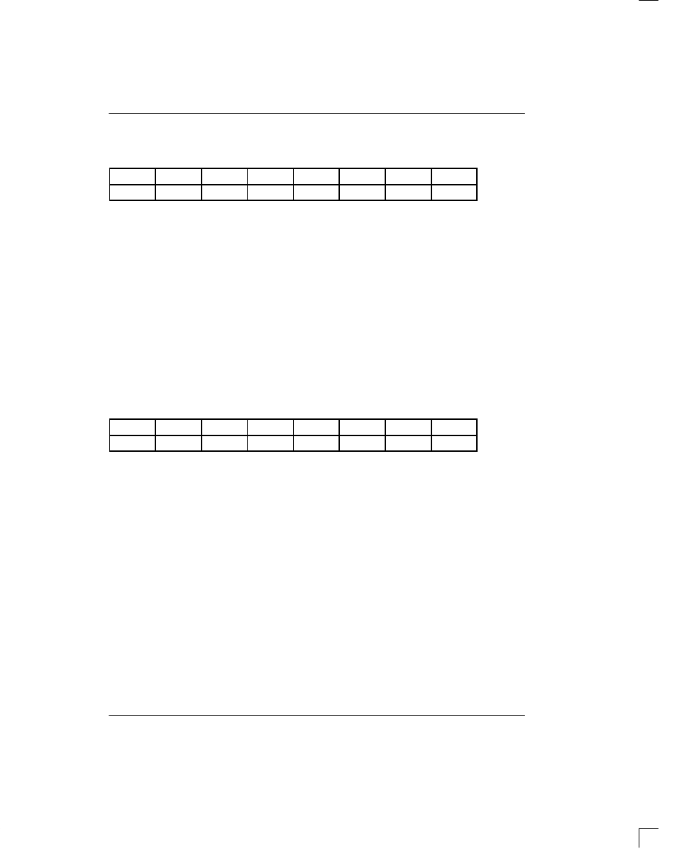
EBCR1: E–BIT COUNT REGISTER 1 (Address=04 Hex)
EBCR2: E–BIT COUNT REGISTER 2 (Address=05 Hex)
(MSB)
(LSB)
(note 1)
(note 1)
(note 1)
(note 1)
(note 1)
(note 1)
EB9
EB8
EB7
EB6
EB5
EB4
EB3
EB2
EB1
EB0
SYMBOL
POSITION
NAME AND DESCRIPTION
EB9
EBCR1.1
MSB of the 10–bit E–Bit count
EB0
EBCR2.0
LSB of the 10–bit E–Bit count
NOTES:
1. The upper six bits of EBCR1 at address 04 are the least significant bits of the 12–bit FAS error counter.
5.4 FAS Bit Error Counter
FAS Count Register 1 (FASCR1) is the most significant
word and FASCR2 is the least significant word of a
12–bit counter that records word errors in the Frame
Alignment Signal in timeslot 0. This counter is disabled
during loss of frame synchronization conditions, it is not
disabled during loss of synchronization at either the
CAS or CRC4 multiframe level. Since the maximum
FAS word error count in a one second period is 4000,
this counter cannot saturate.
FASCR1: FAS BIT COUNT REGISTER 1 (Address=02 Hex)
FASCR2: FAS BIT COUNT REGISTER 2 (Address=04 Hex)
(MSB)
(LSB)
FAS11
FAS10
FAS9
FAS8
FAS7
FAS6
(note 2)
(note 2)
FAS5
FAS4
FAS3
FAS2
FAS1
FAS0
(note 1)
(note 1)
SYMBOL
POSITION
NAME AND DESCRIPTION
FAS11
FASCR1.7
MSB of the 12–bit FAS error count
FAS0
FASCR2.2
LSB of the 12–bit FAS error count
NOTES:
1. The lower two bits of FASCR1 at address 02 are the most significant bits of the 10–bit CRC4 error counter.
2. The lower two bits of FASCR2 at address 04 are the most significant bits of the 10–bit E–Bit counter.
6.0 Sa DATA LINK CONTROL AND
OPERATION
The DS2153Q provides for access to the proposed E1
performance monitor data link in the Sa bit positions.
The device allows access to the Sa bits either via a set of
two internal registers (RNAF and TNAF) or via two
external pins (RLINK and TLINK).
On the receive side, the Sa bits are always reported in
the internal RNAF register (see Section 11 for more
details). All five Sa bits are always output at the RLINK
pin. See Section 13 for detailed timing. Via RCR2, the
user can control the RLCLK pin to pulse during any com-
bination of Sa bits. This allows the user to create a clock
that can be used to capture the needed Sa bits.
On the transmit side, the individual Sa bits can be either
sourced from the internal TNAF register (TCR1.6=0) or
from the external TLINK pin. Via TCR2, the DS2153Q
can be programmed to source any combination of the
EBCR1
EBCR2
FASCR1
FASCR2