Rainbow Electronics DS2153Q User Manual
Page 7
DS2153Q
022697 7/48
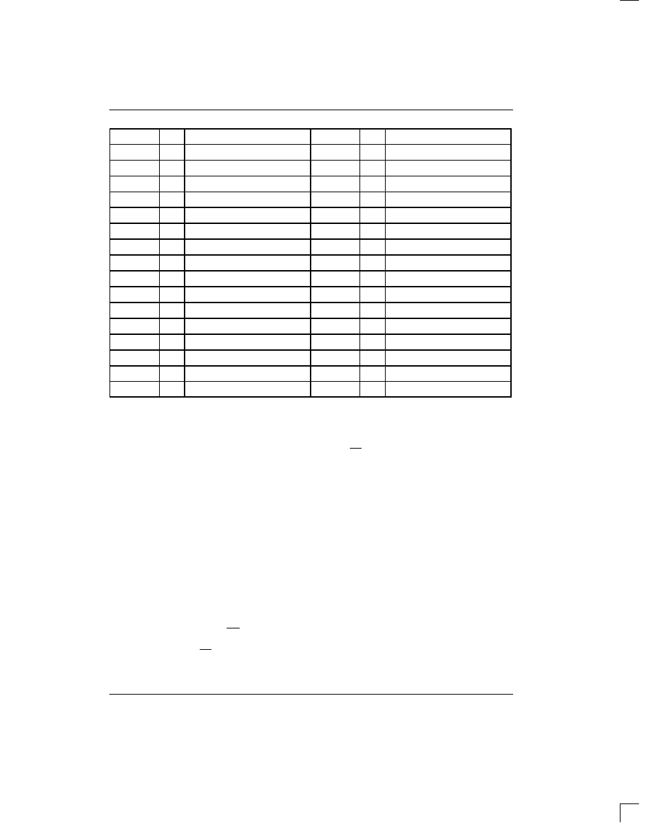
ADDRESS
REGISTER NAME
R/W
ADDRESS
REGISTER NAME
R/W
30
R
Receive Signaling 1
40
R/W
Transmit Signaling 1
31
R
Receive Signaling 2
41
R/W
Transmit Signaling 2
32
R
Receive Signaling 3
42
R/W
Transmit Signaling 3
33
R
Receive Signaling 4
43
R/W
Transmit Signaling 4
34
R
Receive Signaling 5
44
R/W
Transmit Signaling 5
35
R
Receive Signaling 6
45
R/W
Transmit Signaling 6
36
R
Receive Signaling 7
46
R/W
Transmit Signaling 7
37
R
Receive Signaling 8
47
R/W
Transmit Signaling 8
38
R
Receive Signaling 9
48
R/W
Transmit Signaling 9
39
R
Receive Signaling 10
49
R/W
Transmit Signaling 10
3A
R
Receive Signaling 11
4A
R/W
Transmit Signaling 11
3B
R
Receive Signaling 12
4B
R/W
Transmit Signaling 12
3C
R
Receive Signaling 13
4C
R/W
Transmit Signaling 13
3D
R
Receive Signaling 14
4D
R/W
Transmit Signaling 14
3E
R
Receive Signaling 15
4E
R/W
Transmit Signaling 15
3F
R
Receive Signaling 16
4F
R/W
Transmit Signaling 16
Note: the Test Registers 1 and 2 are used only by the factory; these registers must be cleared (set to all zeros) on
power–up initialization to insure proper operation.
2.0 PARALLEL PORT
The DS2153Q is controlled via a mutliplexed bidirec-
tional address/data bus by an external microcontroller
or microprocessor. The DS2153Q can operate with
either Intel or Motorola bus timing configurations. If the
BTS pin is tied low, Intel timing will be selected; if tied
high, Motorola timing will be selected. All Motorola bus
signals are listed in parenthesis (). See the timing dia-
grams in the AC Electrical Characteristics for more
details. The mutliplexed bus on the DS2153Q saves
pins because the address information and data informa-
tion share the same signal paths. The addresses are
presented to the pins in the first portion of the bus cycle
and data will be transferred on the pins during second
portion of the bus cycle. Addresses must be valid prior
to the falling edge of ALE(AS), at which time the
DS2153Q latches the address from the AD0 to AD7
pins. Valid write data must be present and held stable
during the later portion of the DS WR pulses. In a read
cycle, the DS2153Q outputs a byte of data during the
latter portion of the DS or RD pulses. The read cycle is
terminated and the bus returns to a high impedance
state as RD transitions high in Intel timing or as DS tran-
sitions low in Motorola timing.
3.0 CONTROL AND TEST REGISTERS
The operation of the DS2153Q is configured via a set of
seven registers. Typically, the control registers are only
accessed when the system is first powered up. Once
the DS2153Q has been initialized, the control registers
will only need to be accessed when there is a change in
the system configuration. There are two Receive Con-
trol Register (RCR1 and RCR2), two Transmit Control
Registers (TCR1 and TCR2), and three Common Con-
trol Registers (CCR1, CCR2 and CCR3). Each of the
seven registers are described in this section.
The Test Registers at addresses 15 and 19 hex are used
by the factory in testing the DS2153Q. On power–up,
the Test Registers should be set to 00 hex in order for the
DS2153Q to operate properly.