Rainbow Electronics DS2153Q User Manual
Page 5
DS2153Q
022697 5/48
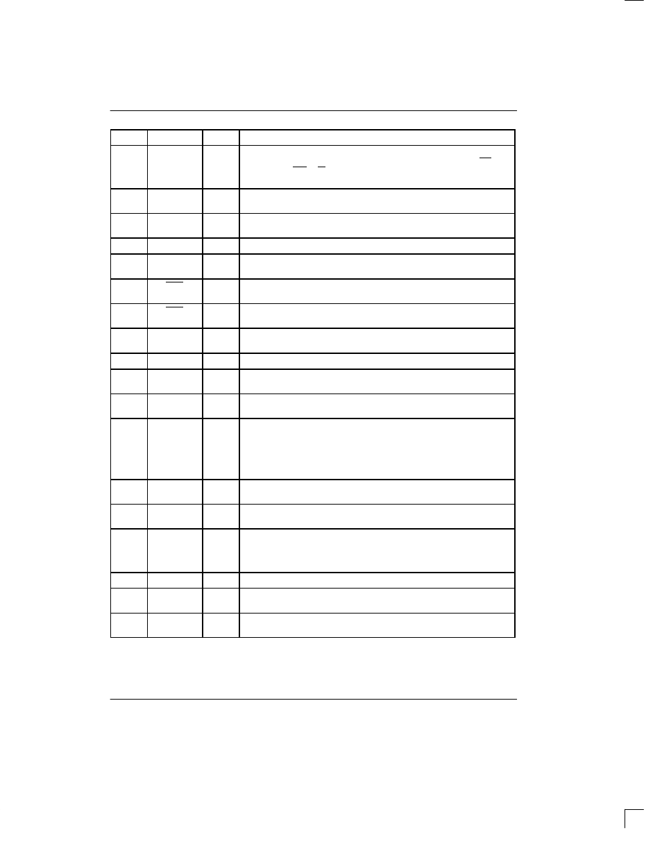
PIN
DESCRIPTION
TYPE
SYMBOL
20
BTS
I
Bus Type Select. Strap high to select Motorola bus timing; strap low to
select Intel bus timing. This pin controls the function of the RD(DS),
ALE(AS), and WR(R/W) pins. If BTS=1, then these pins assume the function
listed in parenthesis ().
21
22
RTIP
RRING
–
Receive Tip and Ring. Analog inputs for clock recovery circuitry; connects
to a 1:1 transformer (see Section 12 for details).
23
RVDD
–
Receive Analog Positive Supply. 5.0 volts. Should be tied to DVDD and
TVDD pins.
24
RVSS
–
Receive Signal Ground. 0.0 volts. Should be tied to local ground plane.
25
26
XTAL1
XTAL2
–
Crystal Connections. A pullable 8.192 MHz crystal must be applied to
these pins. See Section 12 for crystal specifications.
27
INT1
O
Receive Alarm Interrupt 1. Flags host controller during alarm conditions
defined in Status Register 1. Active low, open drain output.
28
INT2
O
Receive Alarm Interrupt 2. Flags host controller during conditions defined
in Status Register 2. Active low, open drain output.
29
TTIP
–
Transmit Tip. Analog line driver output; connects to a step–up transformer
(see Section 12 for details).
30
TVSS
–
Transmit Signal Ground. 0.0 volts. Should be tied to local ground plane.
31
TVDD
–
Transmit Analog Positive Supply. 5.0 volts. Should be tied to DVDD and
RVDD pins.
32
TRING
–
Transmit Ring. Analog line driver outputs; connects to a step–up trans-
former (see Section 12 for details).
33
TCHBLK
O
Transmit Channel Block. A user programmable output that can be forced
high or low during any of the 32 E1 channels. Useful for blocking clocks to
a serial UART or LAPD controller in applications where not all E1 channels
are used such as Fractional E1, 384K bps service (H0), 1920K bps (H12),
or ISDN–PRI. Also useful for locating individual channels in drop–and–insert
applications. See Section 13 for timing details.
34
TLCLK
O
Transmit Link Clock. 4 KHz to 20 KHz demand clock for the TLINK input;
controlled by TCR2. See Section 13 for timing details.
35
TLINK
I
Transmit Link Data. If enabled, this pin will be sampled on the falling edge
of TCLK to insert the Sa bits See Section 13 for timing details.
36
TSYNC
I/O
Transmit Sync. A pulse at this pin will establish either frame or multiframe
boundaries for the DS2153Q. Via TCR1.1, the DS2153Q can be pro-
grammed to output either a frame or multiframe pulse at this pin. See Section
13 for timing details.
37
DVDD
–
Digital Positive Supply. 5.0 volts. Should be tied to RVDD and TVDD pins.
38
TCLK
I
Transmit Clock. 2.048 MHz primary clock. Needed for proper operation of
the parallel control port.
39
TSER
I
Transmit Serial Data. Transmit NRZ serial data, sampled on the falling edge
of TCLK.