Rainbow Electronics DS2153Q User Manual
Page 29
DS2153Q
022697 29/48
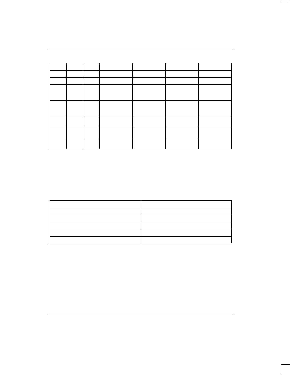
LINE BUILD OUT SELECT IN LICR Table 12–2
L2
L1
L0
APPLICATION
TRANSFORMER
RETURN LOSS
Rt
0
0
0
75 ohm normal
1:1.15 step–up
NM
0 ohms
0
0
1
120 ohm normal
1:1.15 step–up
NM
0 ohms
0
1
0
75 ohm normal
with protection
resistors
1:1.15 step–up
NM
8.2 ohms
0
1
1
120 ohm normal
with protection
resistors
1:1.15 step–up
NM
8.2 ohms
1
0
0
75 ohm with high
return loss
1:1.15 step–up
21 dB
27 ohms
1
1
0
75 ohm with high
return loss
1:1.36 step–up
21 dB
18 ohms
1
0
0
120 ohm with
high return loss
1:1.36 step–up
21 dB
27 ohms
NM=Not Meaningful
Due to the nature of the design of the transmitter in the
DS2153Q, very little jitter (less then 0.00 5UIpp broad-
band from 10 Hz to 100 KHz) is added to the jitter pres-
ent on TCLK. Also, the waveforms that they create are
independent of the duty cycle of TCLK. The transmitter
in the DS2153Q couples to the E1 transmit shielded
twisted pair or COAX via a 1:1.15 or 1:1.36 step up
transformer as shown in Figure 12.1. In order for the
devices to create the proper wavefroms, this trans-
former used must meet the specifications listed in
Table 12.3.
TRANSFORMER SPECIFICATIONS Table 12–3
SPECIFICATION
RECOMMENDED VALUE
Turns Ratio
1:1 (receive) and 1:1.15 or 1:1.36 (transmit)
±
5%
Primary Inductance
600
µ
H minimum
Leakage Inductance
1.0
µ
H maximum
Interwinding Capacitance
60 pF maximum
DC Resistance
1.2 ohms maximum
12.3 Jitter Attenuator
The DS2153Q contains an onboard jitter attenuator that
can be set to a depth of either 32 or 128 bits via the
JABDS bit in the Line Interface Control Register (LICR).
The 128–bit mode is used in applications where large
excursions of wander are expected. The 32–bit mode is
used in delay sensitive applications. The characteris-
tics of the attenuation are shown in Figure 12.4. The jit-
ter attenuator can be placed in either the receive path or
the transmit path by appropriately setting or clearing the
JAS bit in the LICR. Also, the jitter attenuator can be dis-
abled (in effect, removed) by setting the DJA bit in the
LICR. In order for the jitter attenuator to operate prop-
erly, a crystal with the specifications listed in Table 12.4
below must be connected to the XTAL1 and XTAL2 pins.
The jitter attenuator divides the clock provided by the
8.192 MHz crystal at the XTAL1 and XTAL2 pins by to
create an output clock that contains very little jitter.
Onboard circuitry will pull the crystal (by switching in or
out load capacitance) to keep it long term averaged to
the same frequency as the incoming E1 signal. If the
incoming jitter exceeds either 120 UIpp (buffer depth is
128–bits) or 28 UIpp (buffer depth is 32–bits), then the