Figure 7-6, Virtex-5 devices, Implementing external rgmii – Xilinx LOGICORE UG144 User Manual
Page 69: Discontinued product
1-Gigabit Ethernet MAC v8.5 User Guide
69
UG144 April 24, 2009
Implementing External RGMII
R
-- DISCONTINUED PRODUCT --
Virtex-5 Devices
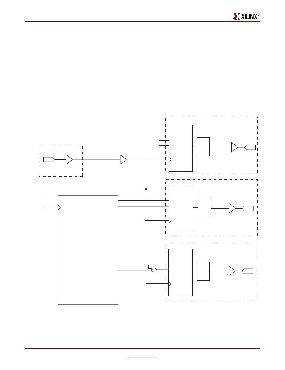
The same logic that is used in
can also be used without modification for Virtex-5
devices. However, an alternative solution has been adopted for the example design
delivered with the core.
shows using the physical transmitter interface of the
core to create an external RGMII in a Virtex-5 device. The signal names and logic shown
exactly match those delivered with the example design when the RGMII is selected.
also shows that the output transmitter signals are registered in the IOBs in
ODDR components. These components convert the input signals into one double-data-rate
signal. The ODDR outputs are passed through IODELAYs—and these can be used to
adjust the relationship between the individual signals. These signals are then output
through OBUFs before being driven to output pads.
Figure 7-6:
External RGMII Transmitter Logic in Virtex-5 Devices
IPAD
IBUFG
IOB LOGIC
gtx_clk
gtx_clk_bufg
IOB LOGIC
1-Gigabit Ethernet MAC Core
gmii_txd_int[0]
gmii_tx_en_int
gmii_tx_er_int
gtx_clk
gmii_txd[0]
gmii_tx_en
gmii_tx_er
IOB LOGIC
rgmii_txd[0]
IOB LOGIC
OBUF
ODDR
OPAD
D1
Q
D2
C
rgmii_tx_ctl
OBUF
ODDR
OPAD
D1
Q
D2
C
rgmii_txc
OBUF
IODELAY
OPAD
gmii_txd_int[4]
gmii_txd[4]
ODDR
D1
Q
D2
C
IODELAY
IODELAY
‘1’
‘0’