Figure 7-5, Chapter 7: using the physical side interface – Xilinx LOGICORE UG144 User Manual
Page 68
68
1-Gigabit Ethernet MAC v8.5 User Guide
UG144 April 24, 2009
Chapter 7: Using the Physical Side Interface
R
-- DISCONTINUED PRODUCT --
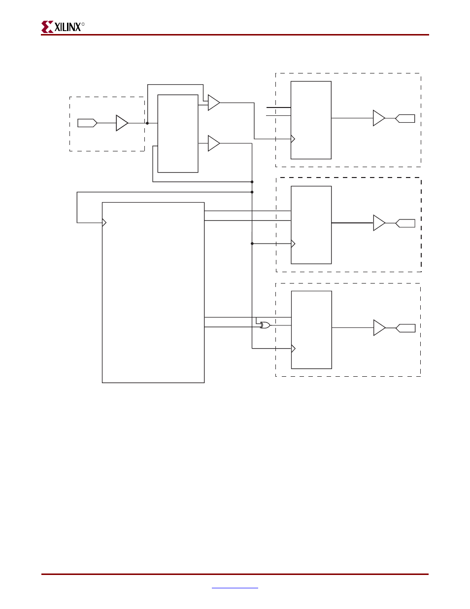
The logic required to forward the transmitter clock is also shown: this uses an ODDR
register so that the clock signal produced incurs exactly on the same delay as the data and
control signals. The rgmii_tx_clk clock signal is phase-shifted by 90 degrees in the
DCM with respect to gtx_clk_bufg. This means that the rising edge of rgmii_txc
occurs in the center of the data valid window—which maximizes setup and hold times
across the interface, as specified in the RGMII v2.0 specification.
The use of the BUFGMUX shown, with one input connected to the DCM CLK90 output is
included so that a reliable 125MHz clock source is always provided on global routing
(when the DCM is held in reset, the DCM input clock is instead selected). This is required
to always provided a reliable clock for the receiver logic DCM: see
Figure 7-5:
External RGMII Transmitter Logic in Virtex-4 Devices
IPAD
IBUFG
IOB LOGIC
gtx_clk
BUFGMUX
gtx_clk_bufg
IOB LOGIC
'1'
'0'
1-Gigabit Ethernet MAC Core
gmii_txd_int[0]
gmii_tx_en_int
gmii_tx_er_int
gtx_clk
gmii_txd[0]
gmii_tx_en
gmii_tx_er
DCM
CLKIN
CLK0
FB
CLK90
rgmii_tx_clk_bufg
IOB LOGIC
rgmii_txd[0]
IOB LOGIC
OBUF
ODDR
OPAD
D1
Q
D2
C
rgmii_tx_ctl
OBUF
ODDR
OPAD
D1
Q
D2
C
rgmii_txc
OBUF
ODDR
OPAD
D1
Q
D2
C
gmii_txd_int[4]
gmii_txd[4]