2 memory protection, 3 bandwidth management, Product preview – Texas Instruments TMS320C6454 User Manual
Page 80
www.ti.com
PRODUCT PREVIEW
5.2 Memory Protection
5.3 Bandwidth Management
TMS320C6454
Fixed-Point Digital Signal Processor
SPRS311A – APRIL 2006 – REVISED DECEMBER 2006
Memory protection allows an operating system to define who or what is authorized to access L1D, L1P,
and L2 memory. To accomplish this, the L1D, L1P, and L2 memories are divided into pages. There are 16
pages of L1P (2KB each), 16 pages of L1D (2KB each), and 16 pages of L2 (64KB each). The L1D, L1P,
and L2 memory controllers in the C64x+ Megamodule are equipped with a set of registers that specify the
permissions for each memory page.
Each page may be assigned with fully orthogonal user and supervisor read, write, and execute
permissions. Additionally, a page may be marked as either (or both) locally or globally accessible. A local
access is a direct CPU access to L1D, L1P, and L2, while a global access is initiated by a DMA (either
IDMA or the EDMA3) or by other system masters. Note that EDMA or IDMA transfers programmed by the
CPU count as global accesses.
The CPU and the system masters on the C6454 device are all assigned a privilege ID of 0. Therefore it is
only possible to specify whether memory pages are locally or globally accessible. The AID0 and LOCAL
bits of the memory protection page attribute registers specify the memory page protection scheme, see
.
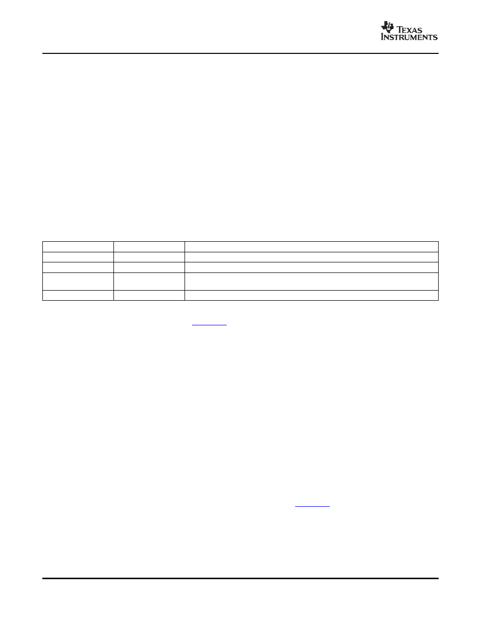
Table 5-1. Available Memory Page Protection Schemes
AID0 Bit
LOCAL Bit
Description
0
0
No access to memory page is permitted.
0
1
Only direct access by CPU is permitted.
1
0
Only accesses by system masters and IDMA are permitted (includes EDMA and IDMA
accesses initiated by the CPU).
1
1
All accesses permitted
For more information on memory protection for L1D, L1P, and L2, see the TMS320C64x+ Megamodule
Reference Guide (literature number
When multiple requestors contend for a single C64x+ Megamodule resource, the conflict is solved by
granting access to the highest priority requestor. The following four resources are managed by the
Bandwidth Management control hardware:
•
Level 1 Program (L1P) SRAM/Cache
•
Level 1 Data (L1D) SRAM/Cache
•
Level 2 (L2) SRAM/Cache
•
Memory-mapped registers configuration bus
The priority level for operations initiated within the C64x+ Megamodule; e.g., CPU-initiated transfers,
user-programmed cache coherency operations, and IDMA-initiated transfers, are declared through
registers in the C64x+ Megamodule. The priority level for operations initiated outside the C64x+
Megamodule by system peripherals is declared through the Priority Allocation Register (PRI_ALLOC), see
. System peripherals with no fields in PRI_ALLOC have their own registers to program their
priorities.
More information on the bandwidth management features of the C64x+ Megamodule can be found in the
TMS320C64x+ Megamodule Reference Guide (literature number
C64x+ Megamodule
80