2 mcbsp electrical data/timing, Product preview – Texas Instruments TMS320C6454 User Manual
Page 180
www.ti.com
PRODUCT PREVIEW
7.13.2 McBSP Electrical Data/Timing
TMS320C6454
Fixed-Point Digital Signal Processor
SPRS311A – APRIL 2006 – REVISED DECEMBER 2006
7.13.2.1
Multichannel Buffered Serial Port (McBSP) Timing
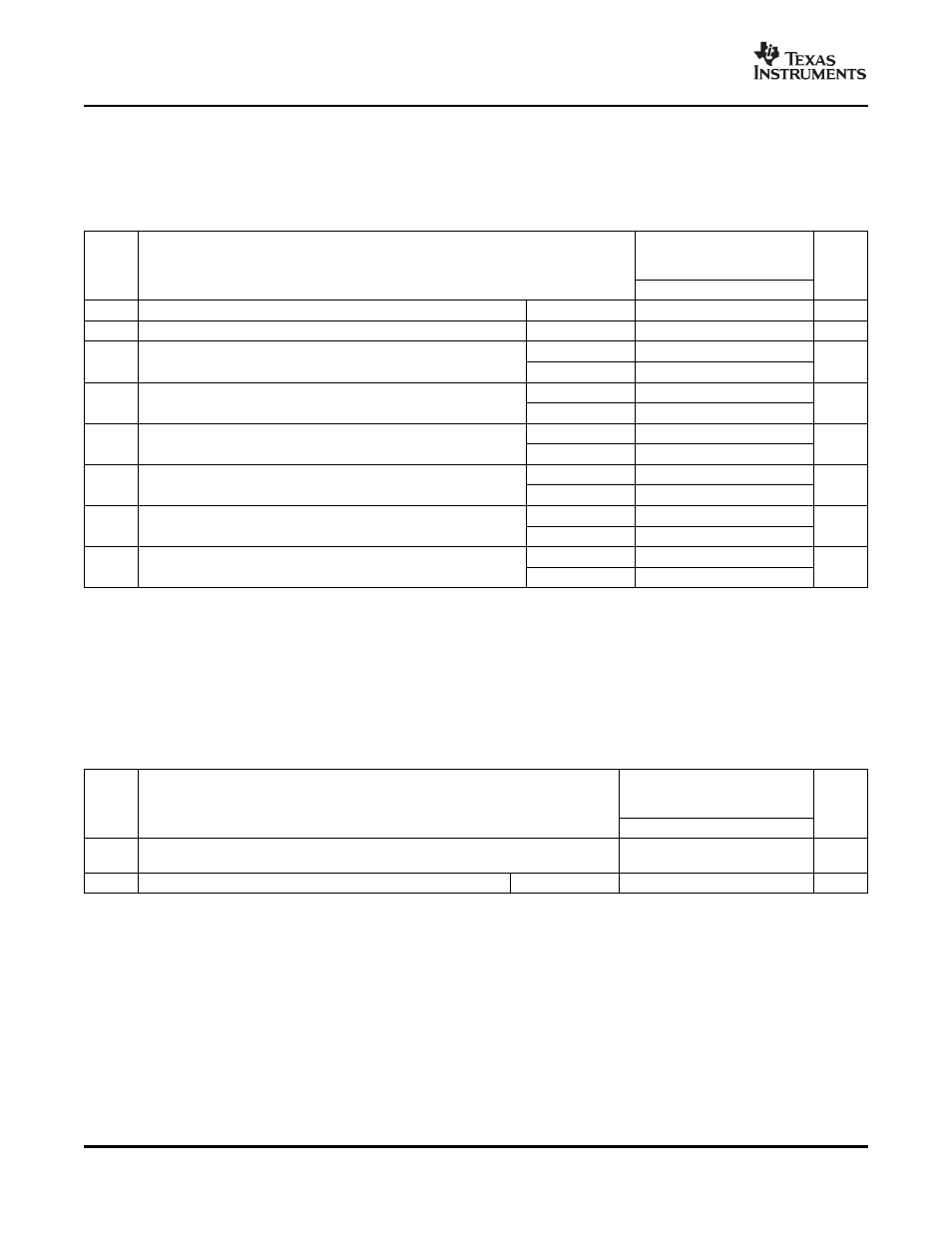
Table 7-59. Timing Requirements for McBSP
(1)
(see
-720
-850
NO.
UNIT
-1000
MIN
MAX
2
t
c(CKRX)
Cycle time, CLKR/X
CLKR/X ext
6P or 10
(2) (3)
ns
3
t
w(CKRX)
Pulse duration, CLKR/X high or CLKR/X low
CLKR/X ext
0.5t
c(CKRX)
– 1
(4)
ns
CLKR int
9
5
t
su(FRH-CKRL)
Setup time, external FSR high before CLKR low
ns
CLKR ext
1.3
CLKR int
6
6
t
h(CKRL-FRH)
Hold time, external FSR high after CLKR low
ns
CLKR ext
3
CLKR int
8
7
t
su(DRV-CKRL)
Setup time, DR valid before CLKR low
ns
CLKR ext
0.9
CLKR int
3
8
t
h(CKRL-DRV)
Hold time, DR valid after CLKR low
ns
CLKR ext
3.1
CLKX int
9
10
t
su(FXH-CKXL)
Setup time, external FSX high before CLKX low
ns
CLKX ext
1.3
CLKX int
6
11
t
h(CKXL-FXH)
Hold time, external FSX high after CLKX low
ns
CLKX ext
3
(1)
CLKRP = CLKXP = FSRP = FSXP = 0. If polarity of any of the signals is inverted, then the timing references of that signal are also
inverted.
(2)
P = 1/CPU clock frequency in ns. For example, when running parts at 1000 MHz, use P = 1 ns.
(3)
Use whichever value is greater. Minimum CLKR/X cycle times must be met, even when CLKR/X is generated by an internal clock
source. The minimum CLKR/X cycle times are based on internal logic speed; the maximum usable speed may be lower due to EDMA
limitations and AC timing requirements.
(4)
This parameter applies to the maximum McBSP frequency. Operate serial clocks (CLKR/X) in the reasonable range of 40/60 duty cycle.
Table 7-60. Switching Characteristics Over Recommended Operating Conditions for McBSP
(1) (2)
(see
-720
-850
NO.
PARAMETER
UNIT
-1000
MIN
MAX
Delay time, CLKS high to CLKR/X high for internal CLKR/X
1
t
d(CKSH-CKRXH)
1.4
10
ns
generated from CLKS input
(3)
2
t
c(CKRX)
Cycle time, CLKR/X
CLKR/X int
6P or 10
(4) (5) (6)
ns
(1)
CLKRP = CLKXP = FSRP = FSXP = 0. If polarity of any of the signals is inverted, then the timing references of that signal are also
inverted.
(2)
Minimum delay times also represent minimum output hold times.
(3)
The CLKS signal is shared by both McBSP0 and McBSP1 on this device.
(4)
Minimum CLKR/X cycle times must be met, even when CLKR/X is generated by an internal clock source. Minimum CLKR/X cycle times
are based on internal logic speed; the maximum usable speed may be lower due to EDMA limitations and AC timing requirements.
(5)
P = 1/CPU clock frequency in ns. For example, when running parts at 1000 MHz, use P = 1 ns.
(6)
Use whichever value is greater.
C64x+ Peripheral Information and Electrical Specifications
180