Product preview – Texas Instruments TMS320C6454 User Manual
Page 134
www.ti.com
PRODUCT PREVIEW
TMS320C6454
Fixed-Point Digital Signal Processor
SPRS311A – APRIL 2006 – REVISED DECEMBER 2006
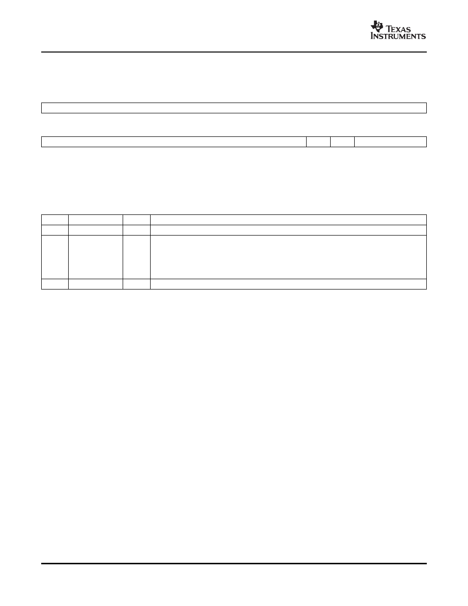
7.7.3.8 PLL Controller Clock Align Control Register
The PLL controller clock align control register (ALNCTL) is shown in
and described in
31
16
Reserved
R-0
15
5
4
3
2
0
Reserved
ALN5
ALN4
Reserved
R-0
R-1
R-1
R-1
LEGEND: R/W = Read/Write; R = Read only; -n = value after reset
Figure 7-18. PLL Controller Clock Align Control Register (ALNCTL) [Hex Address: 029A 0140]
Table 7-26. PLL Controller Clock Align Control Register (ALNCTL) Field Descriptions
Bit
Field
Value
Description
31:5
Reserved
0
Reserved. The reserved bit location is always read as 0. A value written to this field has no effect.
4:3
ALNn
SYSCLKn alignment. Do not change the default values of these fields.
0
Do not align SYSCLKn to other SYSCLKs during GO operation. If SYSn in DCHANGE is set to 1,
SYSCLKn switches to the new ratio immediately after the GOSET bit in PLLCMD is set.
1
Align SYSCLKn to other SYSCLKs selected in ALNCTL when the GOSET bit in PLLCMD is set.
The SYSCLKn ratio is set to the ratio programmed in the RATIO bit in PLLDIVn.
2:0
Reserved
0
Reserved. The reserved bit location is always read as 0. A value written to this field has no effect.
C64x+ Peripheral Information and Electrical Specifications
134