Section 7.7.4, Product preview – Texas Instruments TMS320C6454 User Manual
Page 137
www.ti.com
PRODUCT PREVIEW
7.7.4
PLL1 Controller Input and Output Clock Electrical Data/Timing
CLKIN1
2
3
4
4
5
1
SYSCLK4
3
4
4
2
TMS320C6454
Fixed-Point Digital Signal Processor
SPRS311A – APRIL 2006 – REVISED DECEMBER 2006
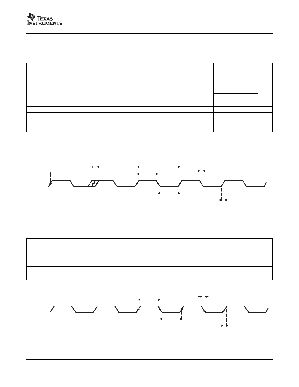
Table 7-29. Timing Requirements for CLKIN1 Devices
(1) (2) (3)
(see
-720
-850
-1000
NO.
PLL MODES
UNIT
x1 (Bypass), x15,
x20, x25, x30, x32
MIN
MAX
1
t
c(CLKIN1)
Cycle time, CLKIN1
(4)
15
30.3
ns
2
t
w(CLKIN1H)
Pulse duration, CLKIN1 high
0.4C
ns
3
t
w(CLKIN1L)
Pulse duration, CLKIN1 low
0.4C
ns
4
t
t(CLKIN1)
Transition time, CLKIN1
1.2
ns
5
t
J(CLKIN1)
Period jitter (peak-to-peak), CLKIN1
100
ps
(1)
The reference points for the rise and fall transitions are measured at 3.3 V V
IL
MAX and V
IH
MIN.
(2)
For more details on the PLL multiplier factors (x1 [BYPASS], x 15, x20, x25, x30, x32), see
, PLL1 Controller Operating
Modes.
(3)
C = CLKIN1 cycle time in ns. For example, when CLKIN1 frequency is 50 MHz, use C = 20 ns.
(4)
The PLL1 multiplier factors (x1 [BYPASS], x 15, x20, x25, x30, x32) further limit the MIN and MAX values for t
c(CLKIN1)
. For more
detailed information on these limitations, see
, Internal Clocks and Maximum Operating Frequencies.
Figure 7-21. CLKIN1 Timing
Table 7-30. Switching Characteristics Over Recommended Operating Conditions for SYSCLK4
[CPU/8 - CPU/12]
(1) (2)
(see
)
-720
-850
NO.
PARAMETER
UNIT
-1000
MIN
MAX
2
t
w(CKO3H)
Pulse duration, SYSCLK4 high
4P – 0.7
6P + 0.7
ns
3
t
w(CKO3L)
Pulse duration, SYSCLK4 low
4P – 0.7
6P + 0.7
ns
4
t
t(CKO3)
Transition time, SYSCLK4
1
ns
(1)
The reference points for the rise and fall transitions are measured at 3.3 V V
OL
MAX and V
OH
MIN.
(2)
P = 1/CPU clock frequency in nanoseconds (ns)
Figure 7-22. SYSCLK4 Timing
C64x+ Peripheral Information and Electrical Specifications
137