Altera Stratix II GX PCI Express Development Board User Manual
Page 41
Altera Corporation
Reference Manual
2–31
August 2006
Stratix II GX PCI Express Development Board
Board Components & Interfaces
The interface to the GigE PHY layer can also use the MII interface for 10
and 100 Mb/s signaling.
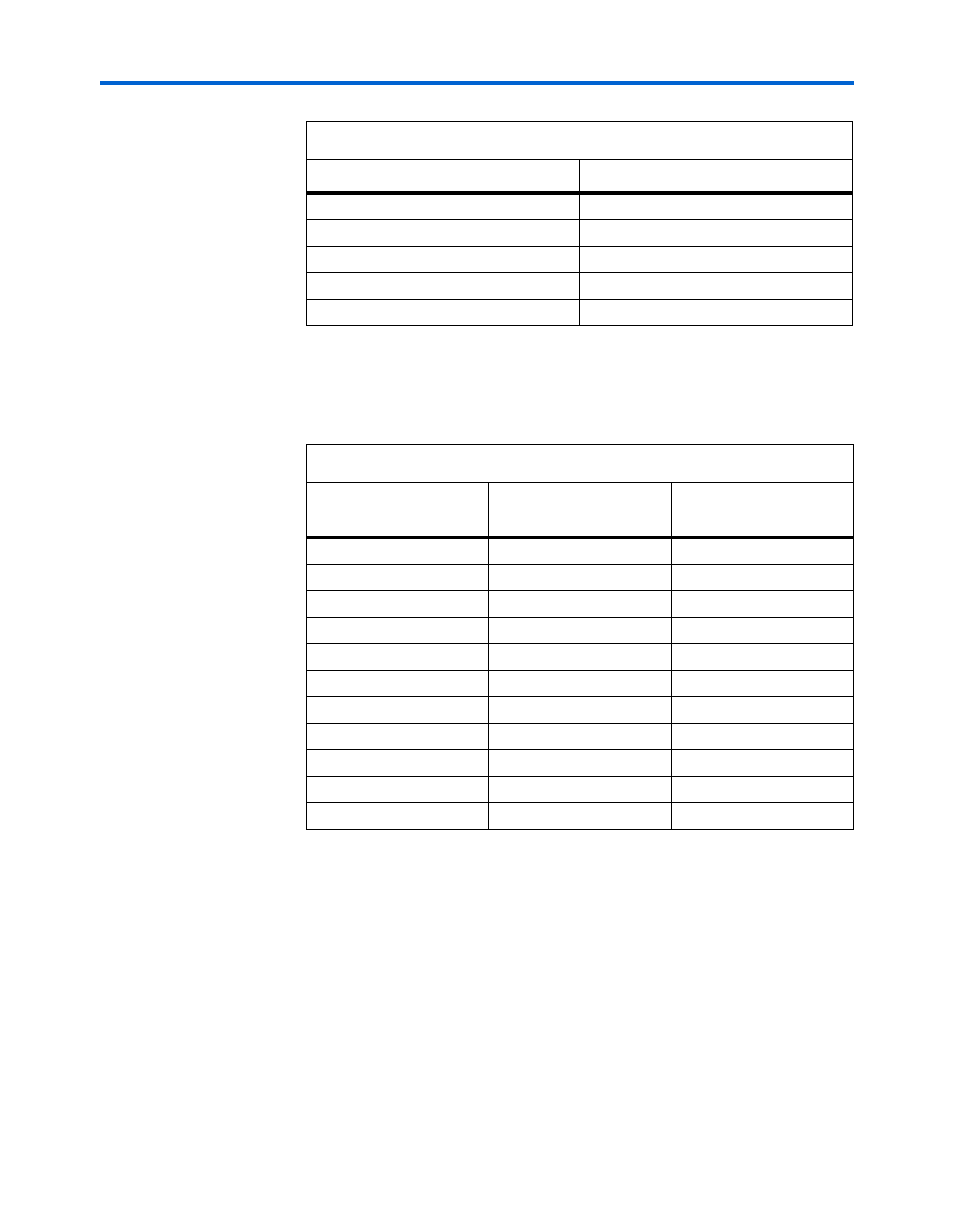
Table 2–24
shows the GMII-to-MII interface
mapping.
The GMII interface is single-data-rate (SDR), source-synchronous in
nature, and operates at 125 MHz. Whereas, the reduced gigabit media
independent interface (RGMII) uses half of the eight data pins, but also
operates at 125 MHz. The RGMII interface achieves the 50% pin count
reduction by using DDR flip flops. The Stratix II GX PCIe development
board can use either the GMII or RGMII interface. However, because of
it’s simpler timing model, the GMII interface is preferred.
enet_txd[3]
C29
enet_txd[4]
D26
enet_txd[5]
J30
enet_txd[6]
F26
enet_txd[7]
F21
Table 2–24. GMII-to-MII I/O Mapping,
Note (1)
Marvel Target
Device Pins
GMII Interface Standard
MII Interface Standard
GTX_CLK
GTX_CLK
—
TX_CLK
—
TX_CLK
TX_ER
TX_ER
TX_ER
TX_EN
TX_EN
TX_EN
TXD[7:0]
TXD[7:0]
TXD[3:0]
RX_CLK
RX_CLK
RX_CLK
RX_ER
RX_ER
RX_ER
RX_DV
RX_DV
RX_DV
RXD[7:0]
RXD[7:0]
RXD[3:0]
CRS
CRS
CRS
COL
COL
COL
Note to
Table 2–24
:
(1)
The 1.8-V logic outputs on the FPGA are up-converted using an FXL4T245
dual-voltage buffer. The 2-5-V CMOS outputs from the Marvel 88E1111 device are
over-driving the FPGA input pins.
Table 2–23. GigE PHY Pin-Out (Part 2 of 2)
Schematic Signal Name
Stratix II GX Device Pin Number