Altera Stratix II GX PCI Express Development Board User Manual
Page 20
2–10
Reference Manual
Altera Corporation
Stratix II GX PCI Express Development Board
August 2006
Featured Device
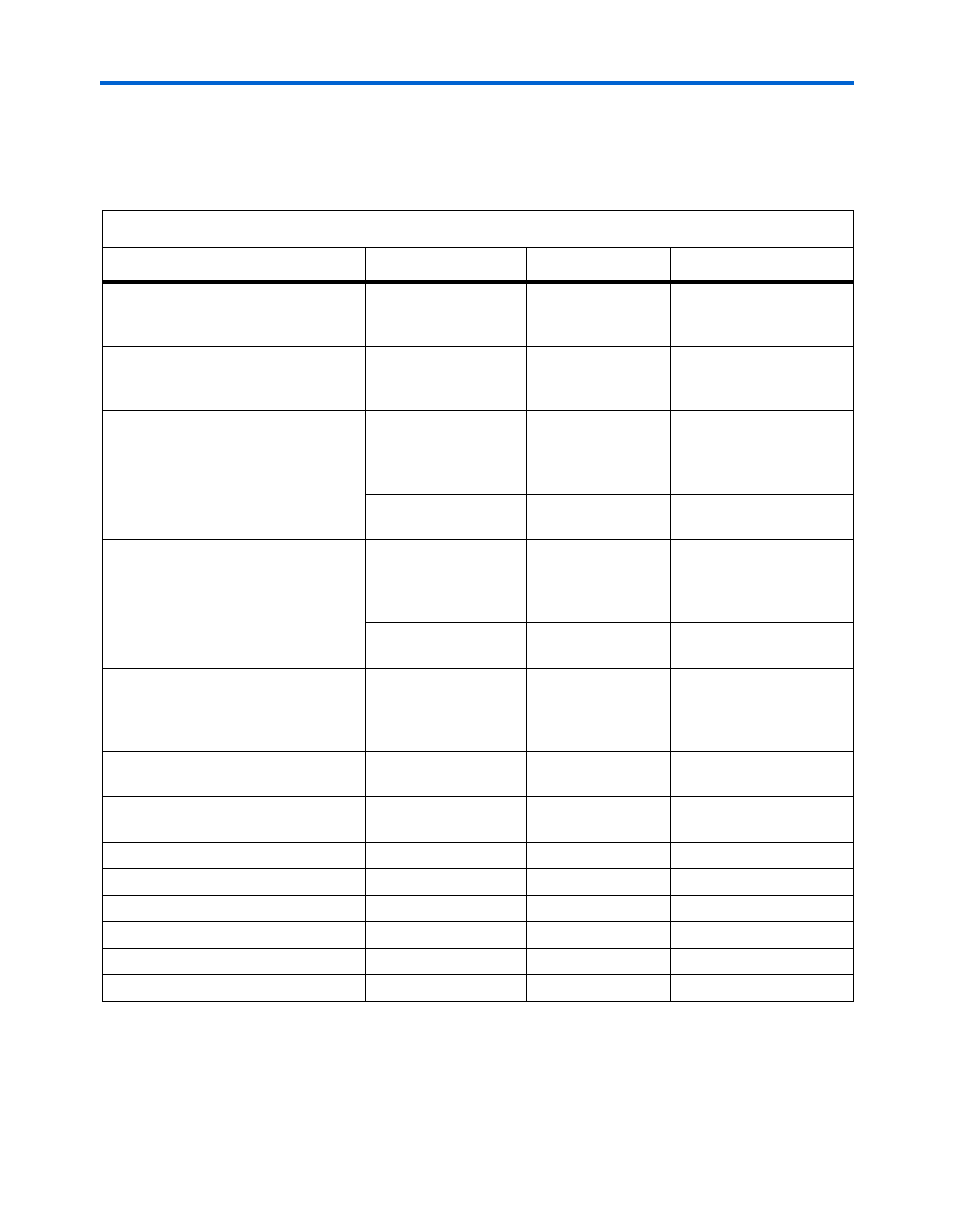
Table 2–3
summarizes Stratix II GX device I/O requirements. Clocks are
noted in a separate column because they sometimes use dedicated I/O
pins or have special needs.
Table 2–3. Stratix II GX Device I/O Requirements Summarized
Function
I/O Type
I/O Count
Clocks
PCIe edge connector
(x8 electrical interface)
1.2-V/1.5-V pseudo
current mode logic
(PCML)
8 XCVR channels
1 LVDS in
Small-form pluggable (SFP)
expansion ports
(2 expansion connectors)
1.2-V/1.5-V PCML
2 XCVR channels
—
High-speed mezzanine card, port A
(XCVRs, LVDS, CMOS)
1.2-V/1.5-V PCML
6 XCVR channels
1 CMOS in
1 CMOS out
2 LVDS in
2 LVDS out
2.5-V CMOS
2.5-V LVDS
84
—
High-speed mezzanine card, port B
(XCVRs, LVDS, CMOS)
1.2-V/1.5-V PCML
4 XCVR channels
1 CMOS in
1 CMOS out
2 LVDS in
2 LVDS out
2.5-V CMOS
2.5-V LVDS
84
—
Gigabit Ethernet (GigE) physical
(PHY) layer
(12-bit,125-MHz Gigabit medium
independent interface [GMII])
2.5-V CMOS
30
1 Out
1 In
DDR2 memory
(72-bit, 333-MHz interface)
1.8-V SSTL
122
—
Quad data rate (QDRII) memory
(36-bit, 300-MHz interface)
1.8-V HSTL
101
—
Flash
2.5-V CMOS
70
—
Push buttons
2.5-V CMOS
3
—
DIP switches
2.5-V CMOS
8
—
LEDs
2.5-V CMOS
18
—
EPLL
clock inputs
2.5-V CMOS
—
2 In
REFCLK
inputs
LVDS
—
3 In
Note to
:
(1)
High-speed mezzanine card, port B: Four XCVR channels are only available with EP2SGX130GF1508 devices.