Altera Stratix II GX PCI Express Development Board User Manual
Page 12

2–2
Reference Manual
Altera Corporation
Stratix II GX PCI Express Development Board
August 2006
Board Overview
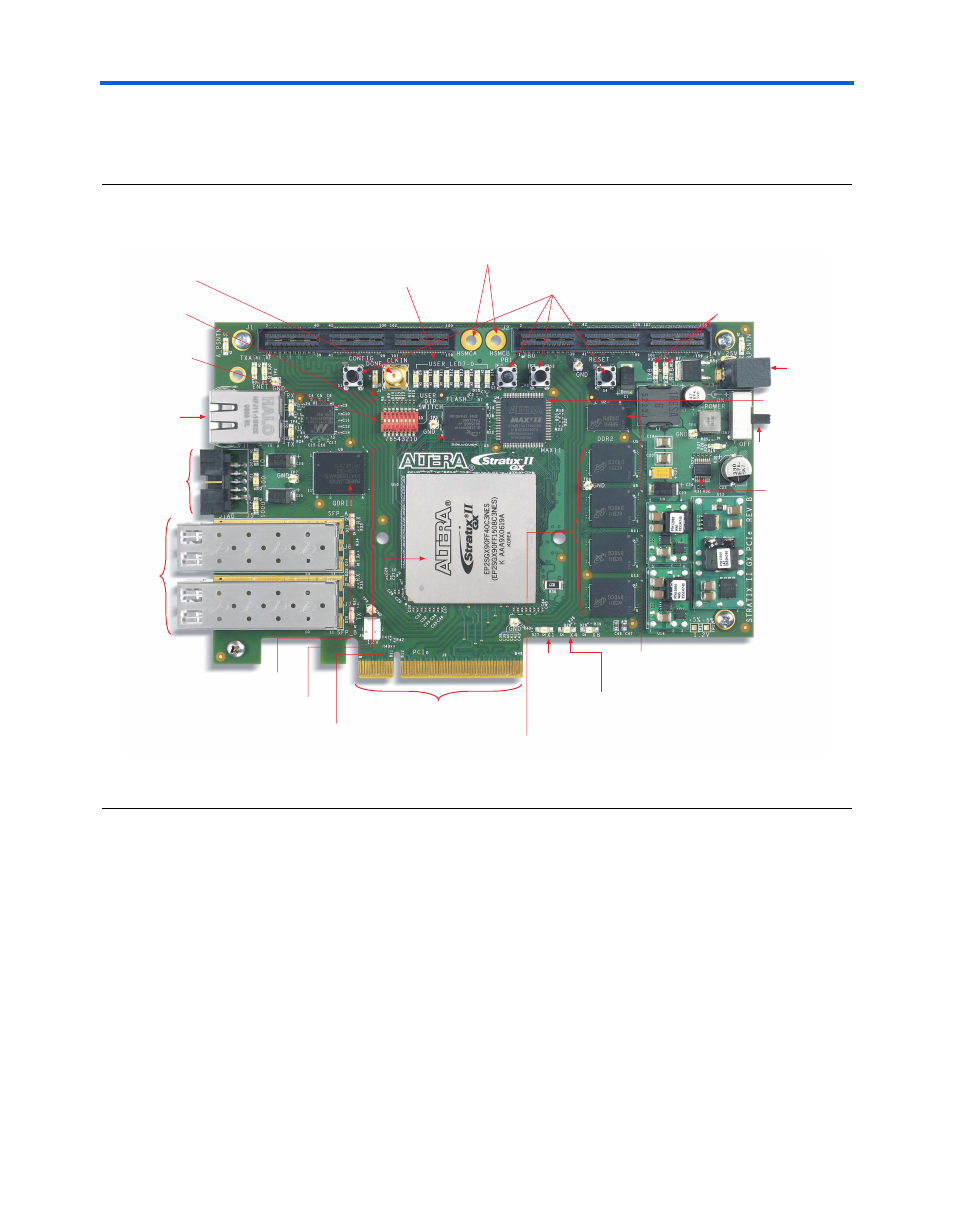
Figure 2–1
shows the top view of the Stratix II GX PCIe development
board.
Figure 2–1. Top View of the Stratix II GX PCIe Development Board
Stratix II GX Device (U10)
Power Switch
(SW1)
Power Supply
Input (J3)
User DIP Switch
Bank (S5)
Flash Device (U3)
User LEDs
(D9 through D16)
MAX II Device
(U4)
High-Speed Mezzanine
Card Interfaces A & B
(J1 and J2)
User Push-Button
Switches (S1 - S4)
DDR2 32 x 16 Mbytes
SDRAM (U5, U8, U11, U13)
Transmit/Receive
Yellow LEDs
(D5 and D6)
DDR2 64 x 8 Mbytes
SDRAM (U2)
Temperature
Sensor With
Alarm (U7)
100-MHz
Crystal (X1)
155.25-MHz
Crystal (X4)
PCI Express x8
Edge Connector
QDRII SRAM (U6)
SFP Ports
A and B
(J6, J7)
JTAG
Header
(J5)
Ethernet RJ-45
Single Port
(RJ1)
HSMC Interface A (J1)
HSMC Interface B (J2)
Configuration Done
LED (D8)
External Clock Input
SMA Connector (J4)
- MAX 10 JTAG (15 pages)
- MAX 10 Power (21 pages)
- Unique Chip ID (12 pages)
- Remote Update IP Core (43 pages)
- Device-Specific Power Delivery Network (28 pages)
- Device-Specific Power Delivery Network (32 pages)
- Hybrid Memory Cube Controller (69 pages)
- ALTDQ_DQS IP (117 pages)
- MAX 10 Embedded Memory (71 pages)
- MAX 10 Embedded Multipliers (37 pages)
- MAX 10 Clocking and PLL (86 pages)
- MAX 10 FPGA (26 pages)
- MAX 10 FPGA (56 pages)
- USB-Blaster II (22 pages)
- GPIO (22 pages)
- LVDS SERDES (27 pages)
- User Flash Memory (33 pages)
- ALTDQ_DQS2 (100 pages)
- Avalon Tri-State Conduit Components (18 pages)
- Cyclone V Avalon-MM (166 pages)
- Cyclone III FPGA Starter Kit (36 pages)
- Cyclone V Avalon-ST (248 pages)
- Stratix V Avalon-ST (286 pages)
- Stratix V Avalon-ST (293 pages)
- DDR3 SDRAM High-Performance Controller and ALTMEMPHY IP (10 pages)
- Arria 10 Avalon-ST (275 pages)
- Avalon Verification IP Suite (224 pages)
- Avalon Verification IP Suite (178 pages)
- FFT MegaCore Function (50 pages)
- DDR2 SDRAM High-Performance Controllers and ALTMEMPHY IP (140 pages)
- Floating-Point (157 pages)
- Integer Arithmetic IP (157 pages)
- Embedded Peripherals IP (336 pages)
- JESD204B IP (158 pages)
- Low Latency Ethernet 10G MAC (109 pages)
- LVDS SERDES Transmitter / Receiver (72 pages)
- Nios II Embedded Evaluation Kit Cyclone III Edition (3 pages)
- Nios II Embedded Evaluation Kit Cyclone III Edition (80 pages)
- IP Compiler for PCI Express (372 pages)
- Parallel Flash Loader IP (57 pages)
- Nios II C2H Compiler (138 pages)
- RAM-Based Shift Register (26 pages)
- RAM Initializer (36 pages)
- Phase-Locked Loop Reconfiguration IP Core (51 pages)
- DCFIFO (28 pages)
