Advanced clocking mode, And the, Related information – Altera SerialLite III Streaming MegaCore Function User Manual
Page 37
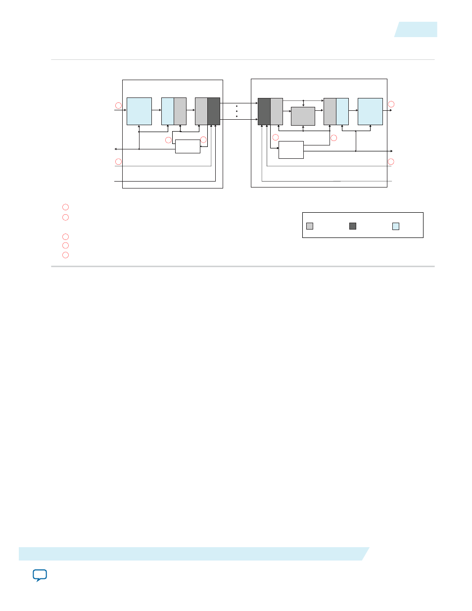
Figure 4-8: SerialLite III Streaming IP Core Block Diagram in Standard Clocking Mode
SerialLite III
Streaming Link
SerialLite III
Streaming Sink Core
Lane Alignment
Module
Adaptation
Module
Application
Module
Sink
User
Interface
Clock
Generator
Sink
User Clock
Transceiver
Reference Clock
Application
Module
Adaptation
Module
SerialLite III
Streaming Source Core
Source
User
Interface
Clock
Generator
Source
User Clock
Transceiver
Reconfiguration
Clock
Transceiver
Reconfiguration
Clock
Core Clock
Core Clock
1
1
4
4
3
3
2
2
For data rates ≤ 15.625 Gbps (Arria 10, Stratix V, and Arria V GZ devices), the Native PHY or Interlaken PHY IP core generates a clock
(serial data rate / 40), that is used as the fPLL reference clock. For data rates > 15.625 Gbps and ≤ 17.4 Gbps, (Arria 10 devices), the
Native PHY or Interlaken PHY IP core generates a clock (serial data rate /64), that is used as the fPLL reference clock.
The fPLL generates the source user and core clocks.
The source and sink user interfaces are driven through the fPLL generated user clock.
For Stratix V and Arria V GZ devices, the transceiver reference clock is provided to the Interlaken PHY IP core.
For Arria 10 devices, the transmit serial clock (tx_serial_clk) is provided to the Native PHY IP Core for TX only.
Transceiver Reference Clock
or Transmit Serial Clock
Core Clock
Domain
Transceiver
Clock Domain
User Clock
Domain
Legend
5
For RX into the Native PHY or Interlaken PHY IP core, the transceiver reference clock is only provided as a parameter.
5
2
3
4
Native PHY or
Interlaken PHY
IP Core
Native PHY or
Interlaken PHY
IP Core
Note: The SerialLite III Streaming IP core uses the transmit serial clock bus (
tx_serial_clk
) and the
tx_pll_locked
signal to connect the external transmit PLL to the Arria 10 Native PHY IP core.
Related Information
Transmission Overheads and Lane Rate Calculations
on page 4-15
Advanced Clocking Mode
The advanced clocking mode allows the user to use a user-specified clock to interface with the source
core. This mode is useful when PPM differences between the user clock (generated by the fPLL) and the
user's interface clock are intolerable. In the advanced clocking mode, the source core is generated with the
PPM-absorption FIFO wrapper module.
Similar to the standard clocking mode, you must specify the user clock frequency through the SerialLite
III Streaming parameter editor. Based on the user clock frequency value, the Quartus II software automat‐
ically calculates the lane rate and the core clock.
The parameter editor provides guidance in selecting a source user clock frequency that meets the
transceiver data rate constraints. For more information about the lane rate calculation, refer to the
“Transmission Overheads and Lane Rate Calculations” section.
In advanced clocking mode, the core clock is faster than the source user clock when data is inserted in the
core. Therefore, the sink user interface may run out of valid data to transmit. The valid signal at the sink
user interface is deasserted to indicate an absence of data at the sink core since the core clock is greater
than the user clock.
UG-01126
2015.05.04
Advanced Clocking Mode
4-13
SerialLite III Streaming IP Core Functional Description
Altera Corporation