Altera ALTDLL User Manual
Page 45
4–9
Chapter 4: Functional Description
ALTDQ_DQS Megafunction
ALTDLL and ALTDQ_DQS Megafunctions User Guide
© February 2012
Altera Corporation
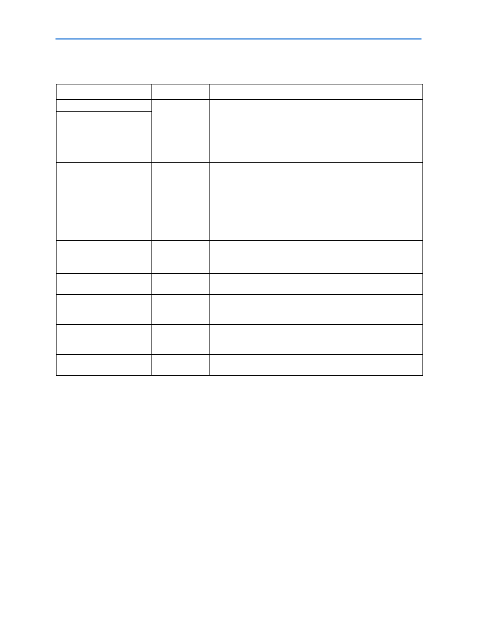
The DQ input path consists of the following blocks:
Table 4–4. DQ Input Path
Block
Name
Description
_INPUT_FF
DQ Input register
blocks
Samples the DQ signal during a read operation. These blocks are
clocked by the core or by a clock pin.
The
_INPUT_FF
block represents a group of flip-flops registers
in the DQ input path.
The
_DDIO_IN
represents a group of double data rate input
registers in the DQ input path.
_DDIO_IN
_IPA_LOW
and
_IPA_HIGH
Input Phase
Alignment (IPA)
Block
Represents the circuitry required to phase shift the input signal. This is
primarily used to match the arrival delay of the DQS (triggered by the
fly-by clock on a DDR3-DIMM) to the latest arrival delay of a DQS from
the DIMM. The input phase alignment block levels or aligns the DQ
group signals in the core using different phase shifts.
For more information about input phase alignment, refer to the Leveling
Circuitry section in the External Memory Interface chapter of the
respective device handbooks.
_HALF_RATE_INPUT
Half-rate input
registers block
Represents the circuitry required to transfer the input signal from a
full-rate clock to a half-rate clock.
Note that this block is only available in Stratix III and Stratix IV devices.
INPUT_DELAY_CHAIN
Input Delay Chain For more information about the input delay chain, refer to
DQS_CONFIG
DQS
Configuration
Block
For more information about the
DQS_CONFIG
block, refer to
.
IO_CONFIG
I/O/
Configuration
Block
For more information about the
IO_CONFIG
block, refer to
IO_CLOCK_DIVIDER
I/O Clock Divider
Block
For more information about I/O clock divider block, refer to