Special function registers specific to the 652x – Maxim Integrated 71M6521BE Energy Meter IC Family Software User Manual
Page 108
71M652X Software User’s Guide
Revision 1.7
TERIDIAN Proprietary
108 of 138
© Copyright 2005-2007 TERIDIAN Semiconductor Corporation
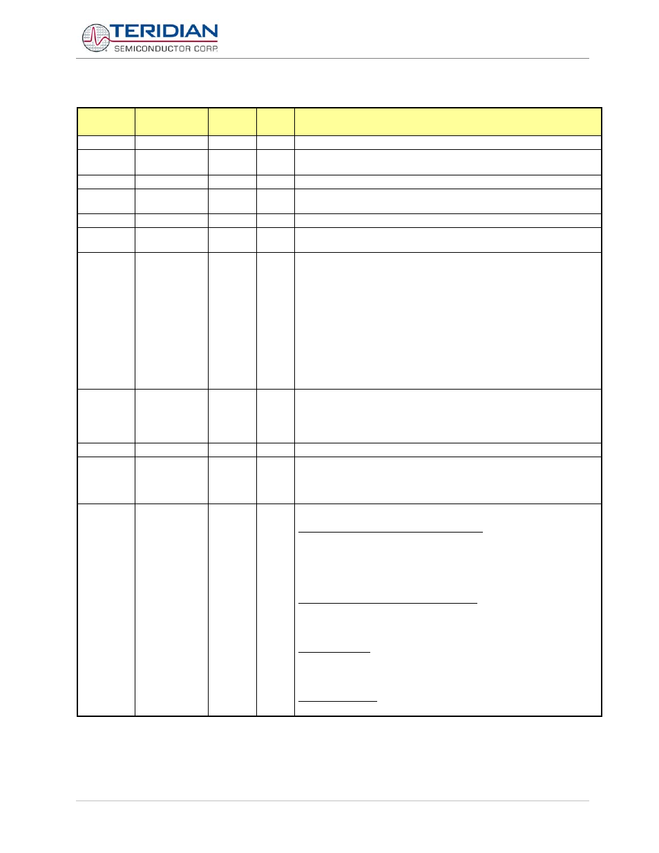
Special Function Registers Specific to the 652X
Register
Alternative
Name
SFR
Address
R/W
Description
DIO0
DIO_0
0x80
R/W
Register for port 0 read and write operations (pins DIO0…DIO7)
DIO8 DIO_DIR0 0xA2
R/W
Data
direction register for port 0. Setting a bit to 1 means that the
corresponding pin is an output.
DIO9
DIO_1
0x90
R/W
Register for port 1 read and write operations (pins DIO8…DIO15)
DIO10
DIO_DIR1
0x91
R/W
Data direction register for port 1. Setting a bit to 1 means that the
corresponding pin is an output.
DIO11
DIO_2
0xA0
R/W
Register for port 2 read and write operations (pins DIO16…DIO21)
DIO12
DIO_DIR2
0xA1
R/W
Data direction register for port 2. Setting a bit to 1 means that the
corresponding pin is an output.
ERASE FLSH_ERASE 0x94 W
This register is used to initiate either the Flash Mass Erase cycle or
the Flash Page Erase cycle. Specific patterns are expected for
FLSH_ERASE in order to initiate the appropriate Erase cycle (default
= 0x00).
0x55 – Initiate Flash Page Erase cycle. Must be proceeded by
a write to FLSH_PGADR @ SFR 0xB7.
0xAA – Initiate Flash Mass Erase cycle. Must be proceeded by a write
to FLSH_MEEN @ sfr 0xB2 and the debug (CC) port must
be enabled.
Any other pattern written to FLSH_ERASE will have no effect.
PGADDR FLSH_PGADR 0xB7 R/W Flash Page Erase Address register containing the flash memory page
address (page 0 thru 127) that will be erased during the Page Erase
cycle. (default = 0x00).
Must be re-written for each new Page Erase cycle.
EEDATA
0x9E
R/W
I2C EEPROM interface data register
EECTRL
0x9F
R/W
I2C EEPROM interface control register. If the MPU wishes to write a
byte of data to EEPROM, it places the data in EEDATA and then
writes the ‘Transmit’ code to EECTRL. The write to EECTRL initiates
the transmit.
FLSHCRL
0xB2
R/W
W
R/W
R
This multi-purpose register contains the following bits:
Bit 0 (FLSH_PWE): Program Write Enable:
0 – MOVX commands refer to XRAM Space, normal operation
(default).
1 – MOVX @DPTR,A moves A to Program Space (Flash) @ DPTR.
This bit is automatically reset after each byte written to flash. Writes to
this bit are inhibited when interrupts are enabled.
Bit 1 (FLSH_MEEN): Mass Erase Enable:
0 – Mass Erase disabled (default).
1 – Mass Erase enabled.
Must be re-written for each new Mass Erase cycle.
Bit 6 (SECURE):
Enables security provisions that prevent external reading of flash
memory and CE program RAM. This bit is reset on chip reset and
may only be set. Attempts to write zero are ignored.
Bit 7 (PREBOOT):
Indicates that the preboot sequence is active.