3 lvds1 voltage selection, Figure 4-4: clear cmos jumper location, Table 4-3: clear cmos jumper settings – IEI Integration KINO-CV-D25501_N26001 User Manual
Page 67
KINO-CV-D25501/N26001 SBC
Page 53
use the jumper cap to close pins 2 and 3 for a few seconds then reinstall the jumper clip
back to pins 1 and 2.
If the “CMOS Settings Wrong” message is displayed during the boot up process, the fault
may be corrected by pressing the F1 to enter the CMOS Setup menu. Do one of the
following:
Enter the correct CMOS setting
Load Optimal Defaults
Load Failsafe Defaults.
After having done one of the above, save the changes and exit the CMOS Setup menu.
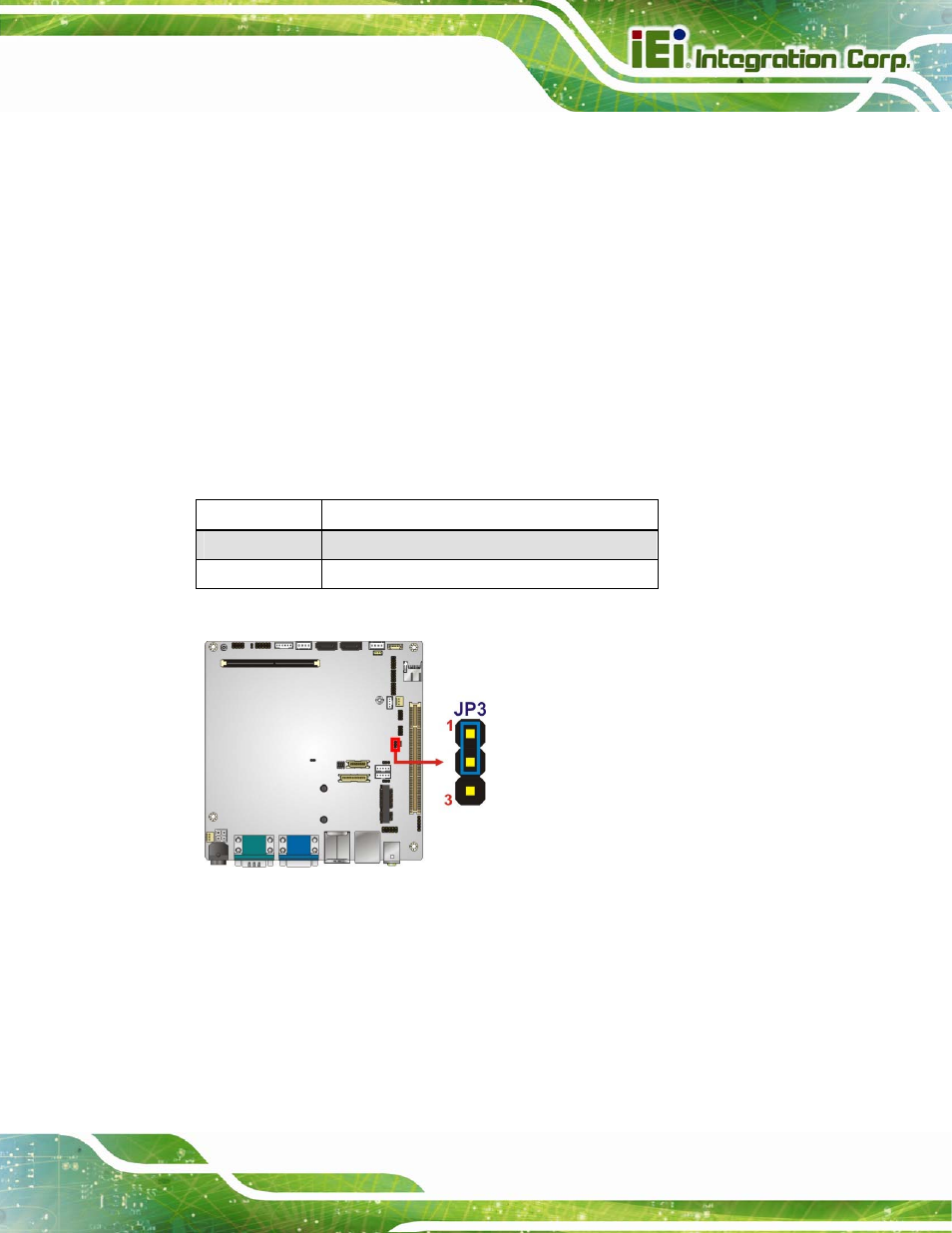
The clear CMOS jumper settings are shown in Table 4-3.
Pin Description
Short 1-2
Keep CMOS Setup (Default)
Short 2-3
Clear CMOS Setup
Table 4-3: Clear CMOS Jumper Settings
Figure 4-4: Clear CMOS Jumper Location
4.5.3 LVDS1 Voltage Selection
Jumper Label:
JP4
Jumper Type:
3-pin header
Jumper Settings:
- SPCIE-5100DX (180 pages)
- SPCIE-C2060 v1.01 (200 pages)
- SPCIE-C2060 v2.12 (212 pages)
- SPCIE-C2160 (204 pages)
- SPCIE-C2260-i2 (217 pages)
- ROCKY-3786 v4.0 (175 pages)
- ROCKY-3786 v4.10 (147 pages)
- PCIE-Q350 v1.00 (272 pages)
- PCIE-Q350 v1.12 (250 pages)
- PCIE-Q350 v1.20 (250 pages)
- PCIE-Q350 v1.30 (213 pages)
- PCIE-Q57A (159 pages)
- PCIE-G41A2 (151 pages)
- PCIE-Q670 v1.03 (206 pages)
- PCIE-Q670 v2.00 (205 pages)
- PCIE-H610 (181 pages)
- PCIE-Q870-i2 (217 pages)
- IOWA-LX-600 (159 pages)
- PCISA-945GSE v1.01 (207 pages)
- PCISA-945GSE v1.10 (190 pages)
- PCISA-9652 v1.00 (232 pages)
- PCISA-9652 v1.01 (232 pages)
- PCISA-PV-D4251_N4551_D5251 (145 pages)
- PICOe-945GSE (197 pages)
- PICOe-GM45A (198 pages)
- PICOe-PV-D4251_N4551_D5251 v1.00 (154 pages)
- PICOe-PV-D4251_N4551_D5251 v1.10 (154 pages)
- PICOe-PV-D4251_N4551_D5251 v1.11 (155 pages)
- PICOe-B650 (156 pages)
- PICOe-HM650 (174 pages)
- HYPER-KBN (139 pages)
- SPXE-14S (3 pages)
- SPXE-9S v1.00 (5 pages)
- SPXE-9S v1.1 (6 pages)
- SPE-9S v1.00 (4 pages)
- SPE-9S v1.1 (5 pages)
- SPE-6S (3 pages)
- SPE-4S (4 pages)
- PE-6SD3 (4 pages)
- PE-6SD2 v4.0 (4 pages)
- PE-6SD2 v2.10 (3 pages)
- PE-6SD (3 pages)
- PE-6S3 v1.0 (2 pages)
- PE-6S3 v4.0 (4 pages)
- PE-6S2 (4 pages)