Phase lock loop (pll), Pll description, Pll programming – Rainbow Electronics AT89C5122 User Manual
Page 42
42
AT8xC5122/23
4202E–SCR–06/06
Phase Lock Loop (PLL)
PLL Description
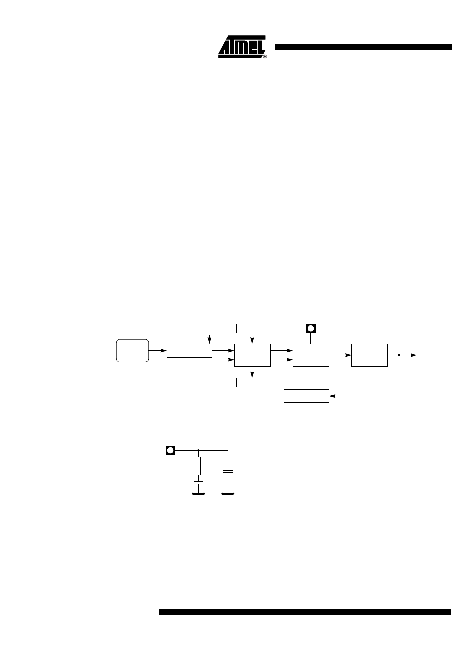
The AT8xC5122/23’s PLL is used to generate internal high frequency clock synchro-
nized with an external low-frequency. Figure 17 shows the internal structure of the PLL.
The PFLD block is the Phase Frequency Comparator and Lock Detector. This block
makes the comparison between the reference clock coming from the N divider and the
reverse clock coming from the R divider and generates some pulses on the Up or Down
signal depending on the edge position of the reverse clock. The PLLEN bit in PLLCON
register is used to enable the clock generation. When the PLL is locked, the bit PLOCK
in PLLCON register is set.
The CHP block is the Charge Pump that generates the voltage reference for the VCO by
injecting or extracting charges from the external filter connected on PLLF pin (see
F i g ur e 18 ). Va lu e of the fi l ter co m p on e nts ar e de ta il e d i n th e Sec tio n “D C
Characteristics”.
The VCO block is the Voltage Controlled Oscillator controlled by the voltage V
REF
pro-
duced by the charge pump. It generates a square wave signal: the PLL clock. The
CK_PLL frequency is defined by the follwing formula:
F
CK_PLL
= F
CK_XTAL1
* (R+1) / (N+1)
Figure 17. PLL Block Diagram and Symbol
Figure 18. PLL Filter Value
PLL Programming
The PLL must be programmed to work at 96 MHz frequency by means of PLLCON and
PLLDIV registers. As soon as the PLL is enabled, the firmware must wait for the lock bit
status to ensure that the PLL is ready.
PLLEN
PLLCON.1
N3:0
N Divider
R divider
VCO
CK_PLL
CK_XTAL1
PFLD
PLOCK
PLLCON.0
PLLF
CHP
V
REF
Up
Down
R3:0
VSS
PLLF
VSS
1,8
K
Ω
150 pF
33 pF