Modes 2 and 3, Transmission (modes 1, 2 and 3), Reception (modes 1, 2 and 3) – Rainbow Electronics AT89C5122 User Manual
Page 132: Framing error detection (modes 1, 2 and 3), Figure 76) c
132
AT8xC5122/23
4202E–SCR–06/06
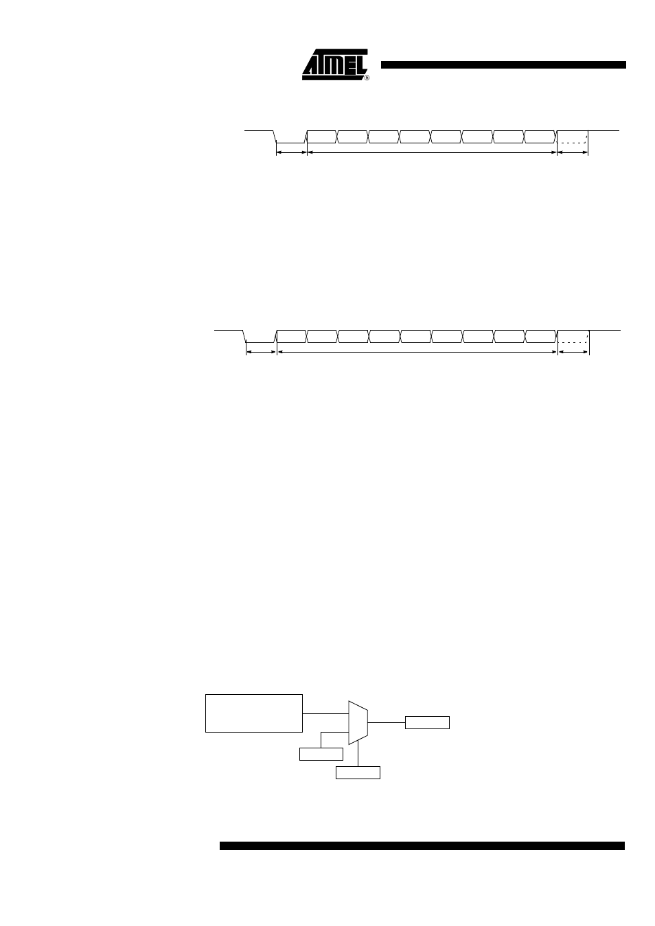
Figure 76. Data Frame Format (Mode 1)
Modes 2 and 3
Modes 2 and 3 are full-duplex, asynchronous modes. The data frame (see Figure 77)
consists of 11 bits: one start bit, eight data bits (transmitted and received LSB first), one
programmable ninth data bit and one stop bit. Serial data is transmitted on the TXD pin
and received on the RXD pin. On receive, the ninth bit is read from RB8 bit in SCON
register. On transmit, the ninth data bit is written to TB8 bit in SCON register. Alterna-
tively, you can use the ninth bit as a command/data flag.
Figure 77. Data Frame Format (Modes 2 and 3)
Transmission
(Modes 1, 2 and 3)
To initiate a transmission, write to SCON register, setting SM0 and SM1 bits according
to Figure 70 on page 130, and setting the ninth bit by writing to TB8 bit. Then, writing the
byte to be transmitted to SBUF register starts the transmission.
Reception
(Modes 1, 2 and 3)
To prepare for a reception, write to SCON register, setting SM0 and SM1 bits according
to Figure 70 on page 130, and setting REN bit. The actual reception is then initiated by a
detected high-to-low transition on the RXD pin.
Framing Error Detection
(Modes 1, 2 and 3)
Framing error detection is provided for the three asynchronous modes. To enable the
framing bit error detection feature, set SMOD0 bit in PCON register as shown in
Figure 78.
When this feature is enabled, the receiver checks each incoming data frame for a valid
stop bit. An invalid stop bit may result from noise on the serial lines or from simultaneous
transmission by two devices. If a valid stop bit is not found, the software sets FE bit in
SCON register.
Software may examine FE bit after each reception to check for data errors. Once set,
only software or a chip reset clear FE bit. Subsequently received frames with valid stop
bits cannot clear FE bit. When the framing error detection feature is enabled, RI rises on
stop bit instead of the last data bit as detailed in Figure 76 and Figure 77.
Figure 78. Framing Error Block Diagram
Mode 1
D0
D1
D2
D3
D4
D5
D6
D7
Start bit
8-bit data
Stop bit
Modes 2 and 3
D0
D1
D2
D3
D4
D5
D6
D8
Start bit
9-bit data
Stop bit
D7
SM0
1
0
SMOD0
PCON.6
SM0/FE
SCON.7
Framing Error
Controller
FE