Transmission (mode 0), Reception (mode 0), Figure 70 – Rainbow Electronics AT89C5122 User Manual
Page 130
130
AT8xC5122/23
4202E–SCR–06/06
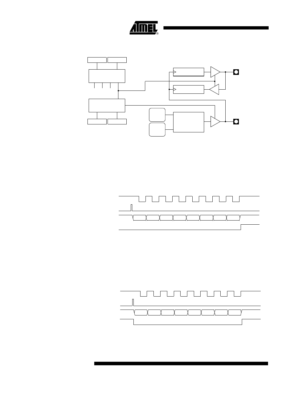
Figure 70. Serial I/O Port Block Diagram (Mode 0)
Transmission (Mode 0)
To start a transmission mode 0, write to SCON register clearing bits SM0, SM1.
As shown in Figure 71, writing the byte to transmit to SBUF register starts the transmis-
sion. Hardware shifts the LSB (D0) onto the RXD pin during the first clock cycle
composed of a high level then low level signal on TXD. During the eighth clock cycle the
MSB (D7) is on the RXD pin. Then, hardware drives the RXD pin high and asserts TI to
indicate the end of the transmission.
Figure 71. Transmission Waveforms (Mode 0)
Reception (Mode 0)
To start a reception in mode 0, write to SCON register clearing SM0, SM1 and RI bits
and setting the REN bit.
As shown in Figure 72, Clock is pulsed and the LSB (D0) is sampled on the RXD pin.
The D0 bit is then shifted into the shift register. After eight sampling, the MSB (D7) is
shifted into the shift register, and hardware asserts RI bit to indicate a completed recep-
tion. Software can then read the received byte from SBUF register.
Figure 72. Reception Waveforms (Mode 0)
IBRG
CLOCK
TXD
RXD
SBUF Tx SR
SBUF Rx SR
SM1
SCON.6
SM0
SCON.7
Mode Decoder
M3 M2 M1 M0
Mode
Controller
RI
SCON.0
TI
SCON.1
CK_
T1
Baud Rate
Controller
Write to SBUF
TXD
RXD
TI
D0
D1
D2
D3
D4
D5
D6
D7
Write to SCON
TXD
RXD
RI
D0
D1
D2
D3
D4
D5
D6
D7
Set REN, Clear RI