Rainbow Electronics ATF1500ABV User Manual
High- performance ee pld atf1500abv, Features, Description
1
Features
•
Operates between 2.7V to 5.5V
•
High-density, High-performance Electrically-erasable Complex
Programmable Logic Device
– 44-pin, 32 I/O CPLD
– 100% connected
– 12 ns Maximum Pin-to-pin Delay
– Registered Operation up to 90.9 MHz
– Fully Connected Input and Feedback Logic Array
•
Flexible Logic Macrocell
– D/T/Latch Configurable Flip-flops
– Global and Individual Register Control Signals
– Global and Individual Output Enable
– Programmable Output Slew Rate
•
Advanced Power Management Features
– Pin-controlled 5 µA Standby Mode (Typical)
– Programmable Pin-keeper Inputs and I/Os
•
Available in Commercial and Industrial Temperature Ranges
•
Available in 44-lead PLCC and TQFP Packages
•
Advanced EEPROM Technology
– 100% Tested
– Completely Reprogrammable
– 10,000 Program/Erase Cycles
– 20-year Data Retention
– 2000V ESD Protection
– 200 mA Latchup Immunity
•
Supported by Popular Third-party Tools
•
Security Fuse Feature
Description
The ATF1500ABV is a high-performance, high-density complex PLD. Built on an
advanced EEPROM technology, it has maximum pin-to-pin delays of 12 ns and sup-
ports sequential logic operation at speeds up to 90.9 MHz. With 32 logic macrocells
and up to 36 inputs, it easily integrates logic from several TTL, SSI, MSI and classic
PLDs.
High-
performance
EE PLD
ATF1500ABV
Rev. 0723I–08/01
TQFP
Top View
1
2
3
4
5
6
7
8
9
10
11
33
32
31
30
29
28
27
26
25
24
23
44
43
42
41
40
39
38
37
36
35
34
12
13
14
15
16
17
18
19
20
21
22
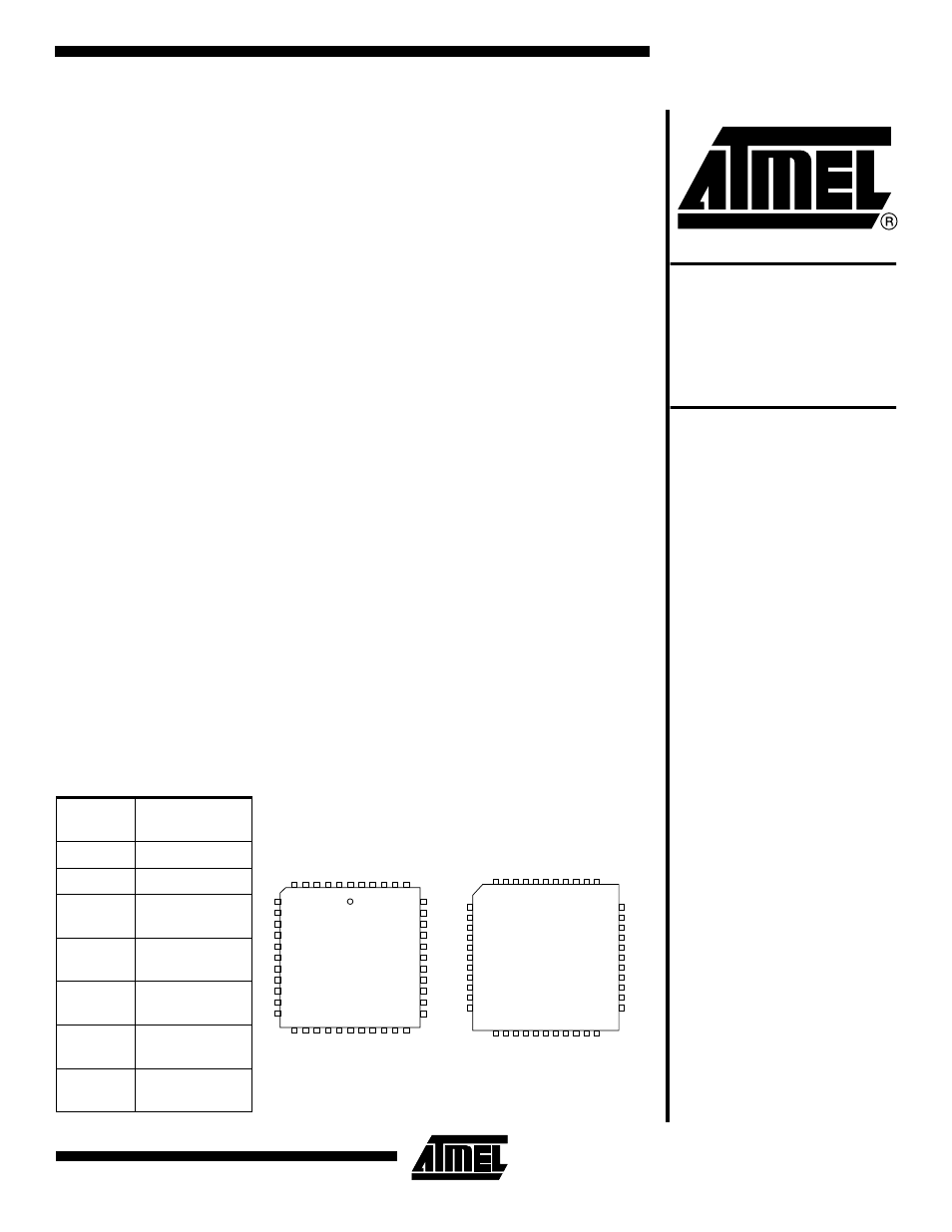
I/O
I/O
I/O
GND
I/O
I/O
I/O
I/O
VCC
I/O
I/O
I/O
I/O
I/O
I/O
VCC
I/O
I/O
I/O
I/O
GND
I/O
I/O
I/O
I/O
I/O
GND
VCC
I/O
I/O
I/O
I/O
I/O
I/O
I/O
I/O/PD
VCC
OE2/I
GCLR/I
OE1/I
CLK/I
GND
I/O
I/O
PLCC
Top View
7
8
9
10
11
12
13
14
15
16
17
39
38
37
36
35
34
33
32
31
30
29
I/O
I/O
I/O
GND
I/O
I/O
I/O
I/O
VCC
I/O
I/O
I/O
I/O
I/O
I/O
VCC
I/O
I/O
I/O
I/O
GND
I/O
6
5
4
3
2
1
44
43
42
41
40
18
19
20
21
22
23
24
25
26
27
28
I/O
I/O
I/O
I/O
GND
VCC
I/O
I/O
I/O
I/O
I/O
I/O
I/O
I/O/PD
VCC
OE2/I
GCLR/I
OE1/I
CLK/I
GND
I/O
I/O
Pin Configurations
Pin
Name
Function
CLK
Clock
I
Logic Inputs
I/O
Bi-directional
Buffers
GCLR
Register Reset
(active low)
OE1,
OE2
Output Enable
(active low)
VCC
(+3V to 5.25V)
Supply
PD
Power-down
(active high)
Document Outline
- Pin Configurations
- Features
- Description
- Functional Logic Diagram(1)
- Bus-friendly Pin-keeper Input and I/Os
- Speed/Power Management
- Input Diagram
- I/O Diagram
- Design Software Support
- ATF1500ABV Macrocell
- ATF1500ABV Macrocell
- Absolute Maximum Ratings*
- DC and AC Operating Conditions
- DC Characteristics
- AC Waveforms
- Register AC Characteristics, Input Pin Clock(1)
- Register AC Characteristics, Product Term Clock(1)
- AC Characteristics(1)
- Power-down AC Characteristics(1)
- Input Test Waveforms and Measurement Levels
- Output Test Load
- Pin Capacitance
- Power-up Reset
- Power-down Mode
- Register Preload
- Output Slew Rate Control
- Security Fuse Usage
- Ordering Information
- Using “C” Product for Industrial