Functional description, Operating modes – Rainbow Electronics AT89C5122 User Manual
Page 139
139
AT8xC5122/23
4202E–SCR–06/06
Functional Description
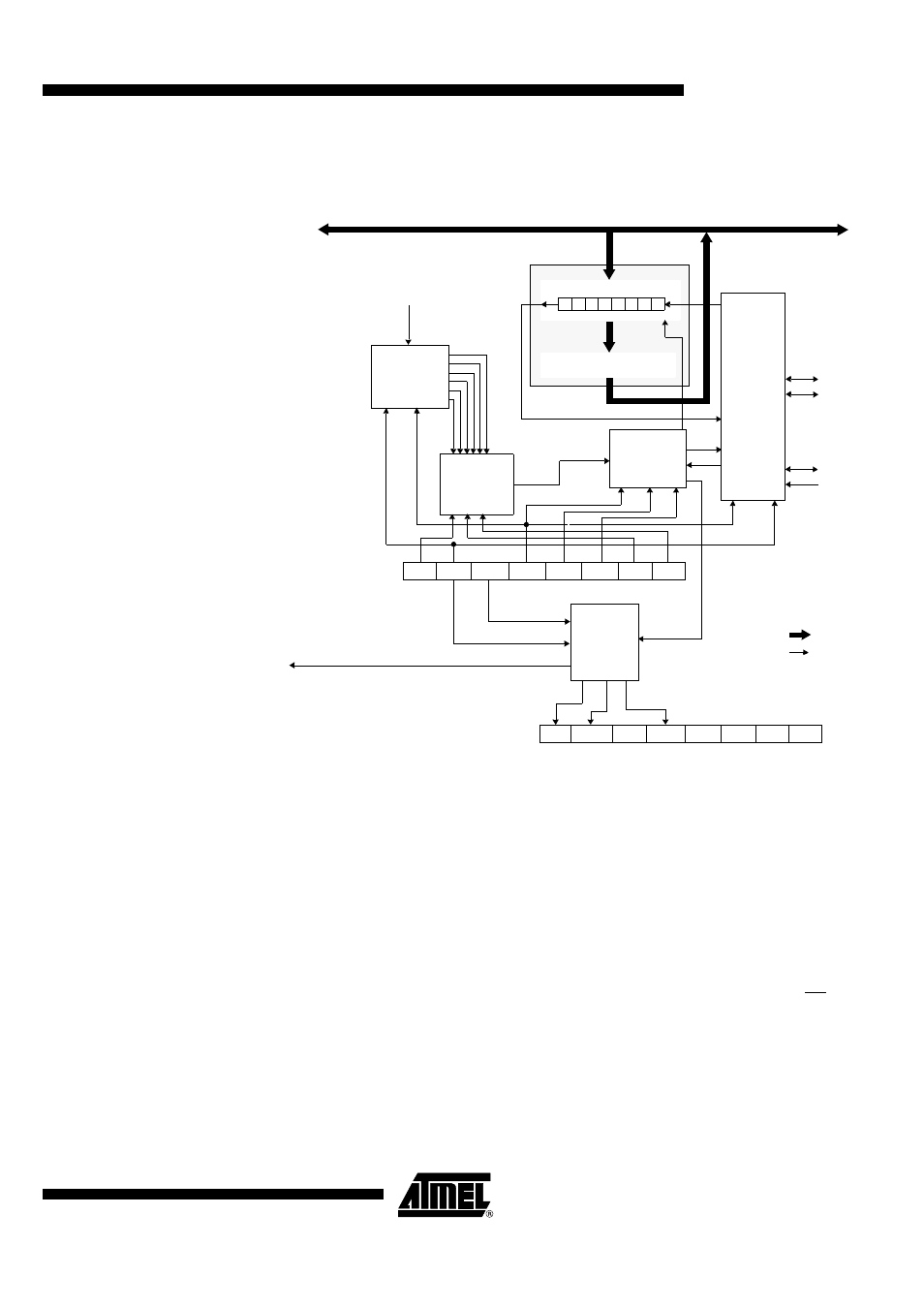
Figure 84 shows a detailed structure of the SPI module.
Figure 84. SPI Module Block Diagram
Operating Modes
The Serial Peripheral Interface can be configured as one of the two modes: Master
mode or Salve mode. The configuration and initialization of the SPI module is made
through one register:
•
The Serial Peripheral Control register (SPCON)
Once the SPI is configured, the data exchange is made using:
•
SPCON
•
The Serial Peripheral Status register (SPSTA)
•
The Serial Peripheral Data register (SPDAT)
During an SPI transmission, data is simultaneously transmitted (shifted out serially) and
received (shifted in serially). A serial clock line (SCK) synchronizes shifting and sam-
pling on the two serial data lines (MOSI and MISO). A Slave Select line (SS) allows
individual selection of a Slave SPI device; Slave devices that are not selected do not
interfere with SPI bus activities.
When the Master device transmits data to the Slave device via the MOSI line, the Slave
device responds by sending data to the Master device via the MISO line. This implies
full-duplex transmission with both data out and data in synchronized with the same clock
(Figure 85).
Shift Register
0
1
2
3
4
5
6
7
Internal Bus
Pin
Control
Logic
MISO
MOSI
SCK
M
S
Clock
Logic
Clock
Divider
Clock
Select
/4
/64
/128
SPI Interrupt Request
8-bit bus
1-bit signal
SS
IntClk
/32
/8
/16
Receive Data Register
SPDAT
SPI
Control
SPSTA
CPHA
SPR0
SPR1
CPOL
MSTR
SSDIS
SPEN
SPR2
SPCON
WCOL
MODF
SPIF
-
-
-
-
-