Rainbow Electronics AT89C5122 User Manual
Page 141
141
AT8xC5122/23
4202E–SCR–06/06
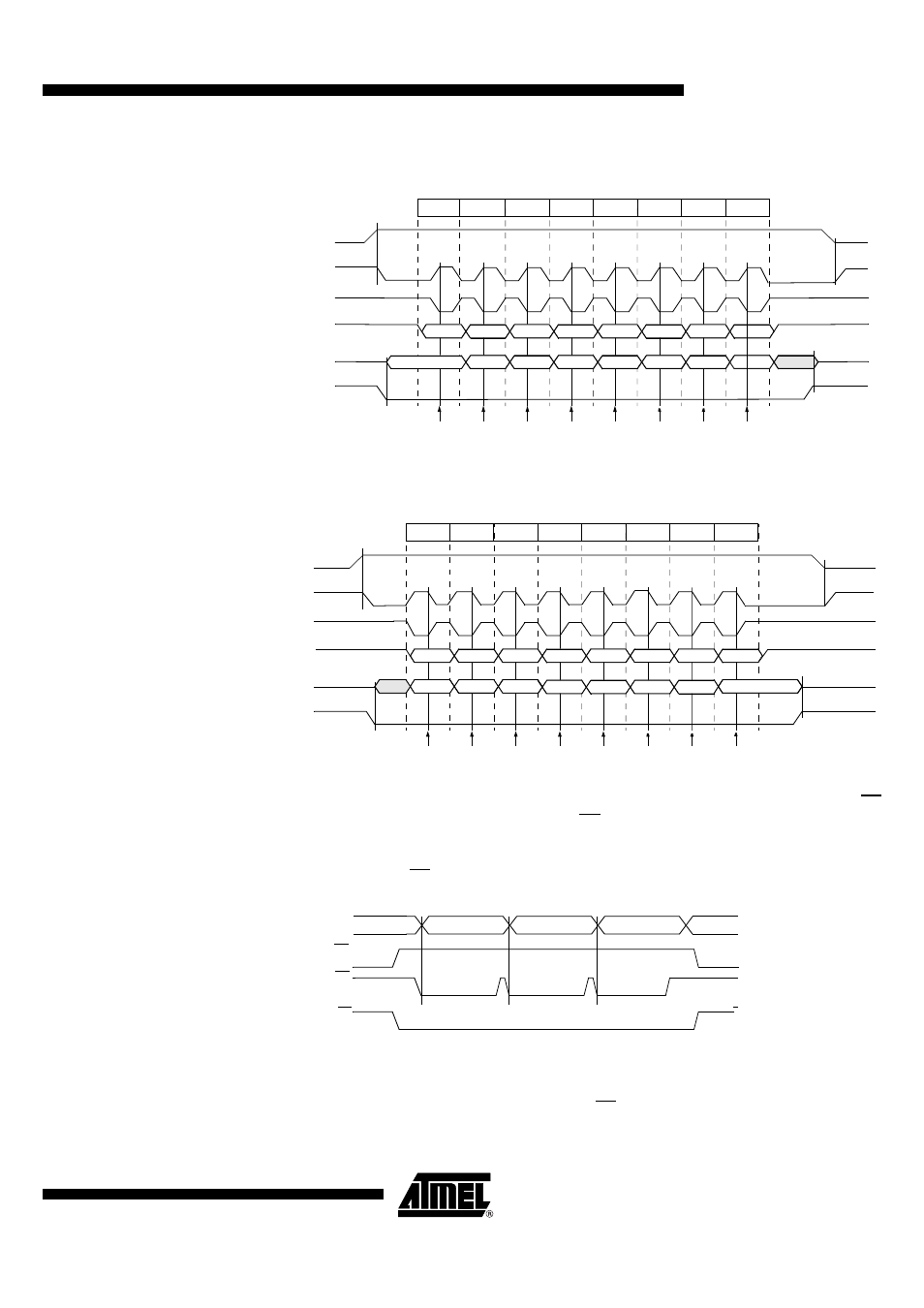
Figure 86. Data Transmission Format (CPHA = 0)
Figure 87. Data Transmission Format (CPHA = 1)
As shown in Figure 86, the first SCK edge is the MSB capture strobe. Therefore the
Slave must begin driving its data before the first SCK edge, and a falling edge on the SS
pin is used to start the transmission. The SS pin must be toggled high and then low
between each byte transmitted (Figure 88).
Figure 88. CPHA/SS Timing
Figure 87 shows an SPI transmission in which CPHA is “1”. In this case, the Master
begins driving its MOSI pin on the first SCK edge. Therefore, the Slave uses the first
SCK edge as a start transmission signal. The SS pin can remain low between transmis-
MSB
bit6
bit5
bit4
bit3
bit2
bit1
LSB
bit6
bit5
bit4
bit3
bit2
bit1
MSB
LSB
1
3
2
4
5
6
7
8
Capture Point
SS (to Slave)
MISO (from Slave)
MOSI (from Master)
SCK (CPOL = 1)
SCK (CPOL = 0)
SPEN (internal)
SCK Cycle Number
MSB
bit6
bit5
bit4
bit3
bit2
bit1
LSB
bit6
bit5
bit4
bit3
bit2
bit1
MSB
LSB
1
3
2
4
5
6
7
8
Capture point
SS (to Slave)
MISO (from Slave)
MOSI (from Master)
SCK (CPOL = 1)
SCK (CPOL = 0)
SPEN (internal)
SCK Cycle Number
Byte 1
Byte 2
Byte 3
MISO/MOSI
Master SS
Slave SS
(CPHA = 1)
Slave SS
(CPHA = 0)