Rainbow Electronics ATV750BL User Manual
Features, Logic diagram description, Pin configurations
1
Features
•
Advanced, High-speed Programmable Logic Device – Superset of 22V10
– Improved Performance - 7.5 ns t
PD
, 95 MHz External Operation
– Enhanced Logic Flexibility
– Backward Compatible with ATV750(L) Software and Hardware
•
New Flip-flop Features
– D- or T-type
– Product Term or Direct Input Pin Clocking
•
High-speed Erasable Programmable Logic Devices
– 7.5 ns Maximum Pin-to-pin Delay
•
Highest Density Programmable Logic Available in a 24-pin Package
•
Increased Logic Flexibility
– 42 Array Inputs, 20 Sum Terms and 20 Flip-flops
•
Enhanced Output Logic Flexibility
– All 20 Flip-flops Feed Back Internally
– 10 Flip-flops are Also Available as Outputs
•
Full Military, Commercial and Industrial Temperature Ranges
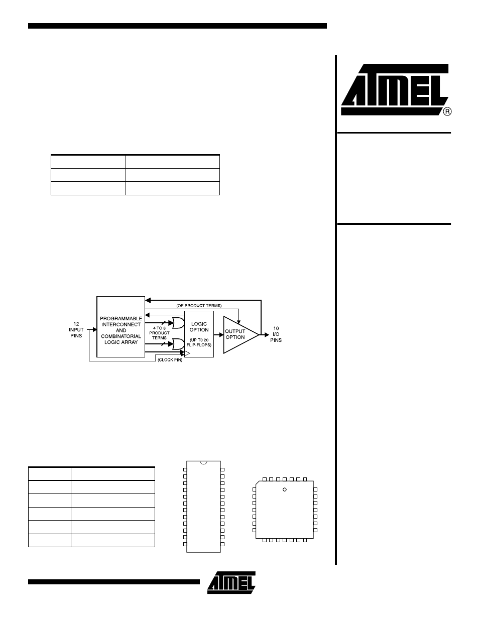
Logic Diagram
Description
The ATV750B(L) is twice as powerful as most other 24-pin programmable logic
devices. Increased product terms, sum terms, flip-flops and output logic configurations
translate into more usable gates. High-speed logic and uniform, predictable delays
guarantee fast in-system performance.
Device
I
CC
, Standby
ATV750B
125 mA
ATV750BL
15 mA
High-speed UV
Erasable
Programmable
Logic Device
ATV750B
ATV750BL
Commercial and
industrial versions
are obsolete. Please
use ATF750C.
Military versions
continue to be available,
but please do not
use for new designs.
For new military
applications, recommend
multiple ATF22V10s.
Rev. 0301I–08/01
Pin Configurations
Pin Name
Function
CLK
Clock
IN
Logic Inputs
I/O
Bi-directional Buffers
*
No Internal Connection
V
CC
+5V Supply
DIP/SOIC
1
2
3
4
5
6
7
8
9
10
11
12
24
23
22
21
20
19
18
17
16
15
14
13
CLK/IN
IN
IN
IN
IN
IN
IN
IN
IN
IN
IN
GND
VCC
I/O
I/O
I/O
I/O
I/O
I/O
I/O
I/O
I/O
I/O
IN
PLCC/LCC
5
6
7
8
9
10
11
25
24
23
22
21
20
19
IN
IN
IN
*
IN
IN
IN
I/O
I/O
I/O
*
I/O
I/O
I/O
4
3
2
1
28
27
26
12
13
14
15
16
17
18
IN
IN
GND
*
IN
I/O
I/O
IN
IN
CLK/IN
*
VCC
I/O
I/O
Document Outline
- Pin Configurations
- Features
- Logic Diagram
- Description
- Absolute Maximum Ratings*
- Clock Mux
- Output Options
- DC and AC Operating Conditions(1)
- DC Characteristics
- Input Test Waveforms and Measurement Levels
- Output Test Load
- AC Waveforms, Product Term Clock(1)
- AC Characteristics, Product Term Clock(1)
- AC Waveforms, Input Pin Clock(1)
- AC Characteristics, Input Pin Clock
- Functional Logic Diagram ATV750B, Upper Half
- Functional Logic Diagram ATV750B, Lower Half
- Preload of Registered Outputs
- Power-up Reset
- Pin Capacitance
- Using the ATV750B(L) Many Advanced Features
- Programming Software Support
- Synchronous Preset and Asynchronous Reset
- Security Fuse Usage
- Erasure Characteristics
- Atmel CMOS PLDs
- Ordering Information
- Using “C” Product for Industrial