Rainbow Electronics AT89C5131 User Manual
Page 9
9
AT89C5131
4136A–USB–03/03
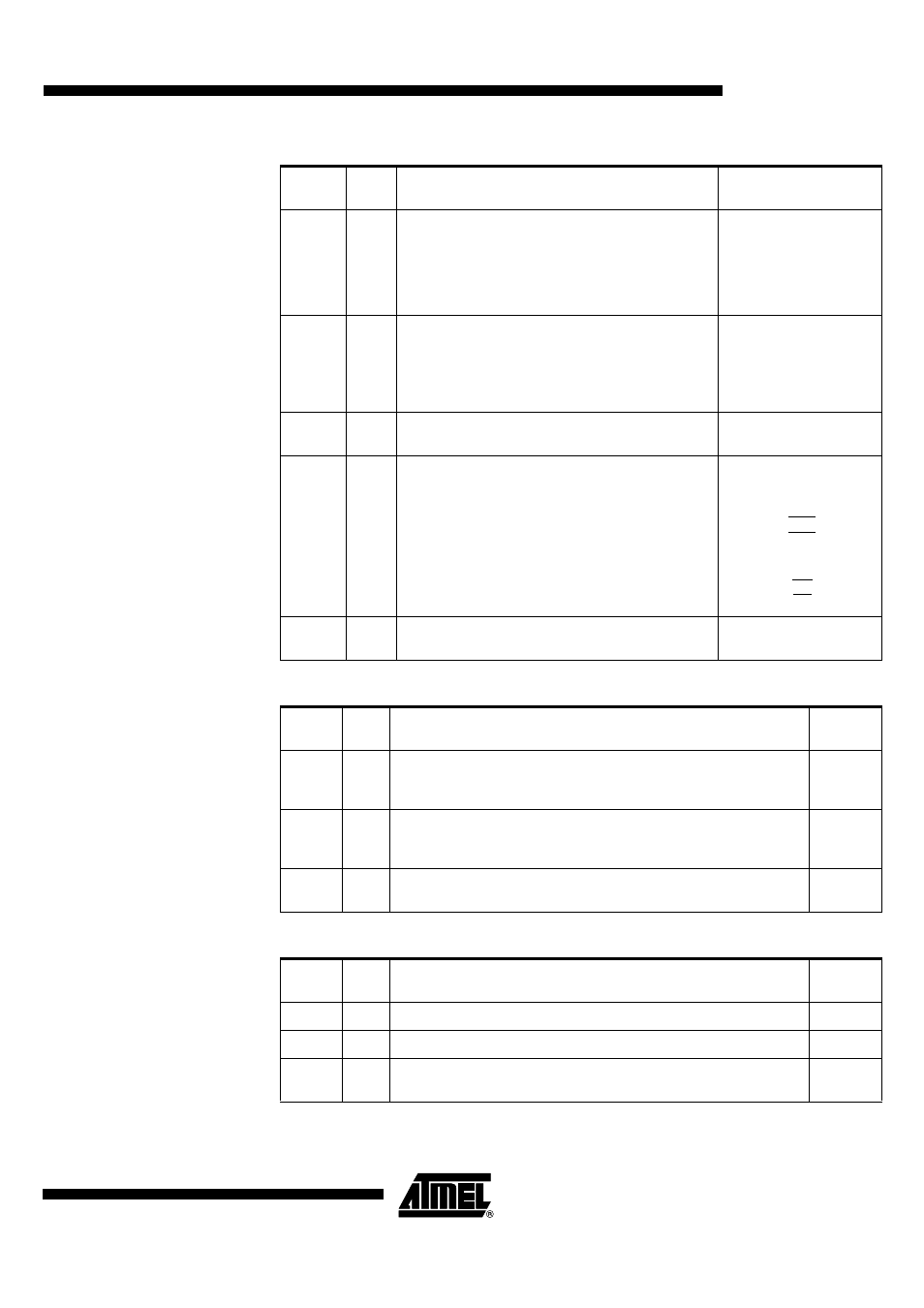
Table 7. Ports Signal Description
Table 8. Clock Signal Description
Table 9. USB Signal Description
Signal
Name
Type
Description
Alternate Function
P0[7:0]
I/O
Port 0
P0 is an 8-bit open-drain bidirectional I/O port. Port 0
pins that have 1s written to them float and can be used
as high impedance inputs. To avoid any parasitic current
consumption, Floating P0 inputs must be pulled to V
DD
or
V
SS
.
AD[7:0]
P1[7:0]
I/O
Port 1
P1 is an 8-bit bidirectional I/O port with internal pull-ups,
except for P1.6 and P1.7 that are true open drain
outputs.
KIN[7:0]
T2
T2EX
ECI
CEX[4:0]
P2[7:0]
I/O
Port 2
P2 is an 8-bit bidirectional I/O port with internal pull-ups.
A[15:8]
P3[7:0]
I/O
Port 3
P3 is an 8-bit bidirectional I/O port with internal pull-ups.
LED[3:0]
RxD
TxD
INT0
INT1
T0
T1
WR
RD
P4[1:0]
I/O
Port 4
P4 is an 2-bit bidirectional I/O port.
Signal
Name
Type
Description
Alternate
Function
XTAL1
I
Input to the on-chip inverting oscillator amplifier
To use the internal oscillator, a crystal/resonator circuit is connected to this
pin. If an external oscillator is used, its output is connected to this pin.
-
XTAL2
O
Output of the on-chip inverting oscillator amplifier
To use the internal oscillator, a crystal/resonator circuit is connected to this
pin. If an external oscillator is used, leave XTAL2 unconnected.
-
PLLF
I
PLL Low Pass Filter input
Receives the RC network of the PLL low pass filter.
-
Signal
Name
Type
Description
Alternate
Function
D+
I/O
USB Data + signal
-
D-
I/O
USB Data - signal
-
VREF
O
USB Reference Voltage
Connect this pin to D+ using a 1.5 k
Ω
resistor to use the Detach function.
-