Clock controller, Introduction, Oscillator – Rainbow Electronics AT89C5131 User Manual
Page 19
19
AT89C5131
4136A–USB–03/03
Clock Controller
Introduction
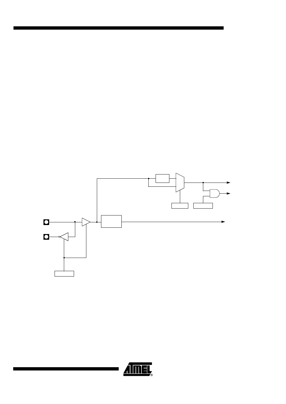
The AT89C5131 clock controller is based on an on-chip oscillator feeding an on-chip
Phase Lock Loop (PLL). All the internal clocks to the peripherals and CPU core are gen-
erated by this controller.
The AT89C5131 X1 and X2 pins are the input and the output of a single-stage on-chip
inverter (see Figure 5) that can be configured with off-chip components as a Pierce
oscillator (see Figure 6). Value of capacitors and crystal characteristics are detailed in
the section “DC Characteristics”.
The clock controller outputs three different clocks as shown in Figure 5:
•
a clock for the CPU core
•
a clock for the peripherals which is used to generate the Timers, PCA, WD, and Port
sampling clocks
•
a clock for the USB controller
These clocks are enabled or disabled depending on the power reduction mode as
detailed in Section “Power Management”, page 145.
Figure 5. Oscillator Block Diagram
Oscillator
Two clock sources are available for CPU:
•
Crystal oscillator on X1 and X2 pins: Up to 32 MHz
In order to optimize the power consumption, the oscillator inverter is inactive when the
PLL output is not selected for the USB device.
X1
X2
PD
PCON.1
IDL
PCON.0
Peripheral
CPU Core
0
1
X2
CKCON.0
÷
2
Clock
Clock
PLL
USB
Clock