Signals – Rainbow Electronics AT89C5131 User Manual
Page 7
7
AT89C5131
4136A–USB–03/03
Signals
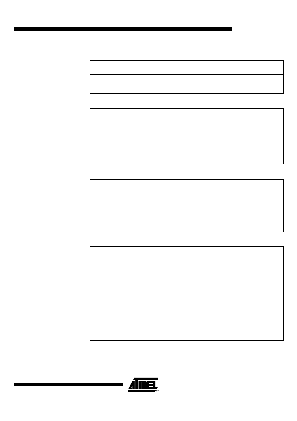
All the AT89C5131 signals are detailed by functionality on Table 1 through Table 11.
Table 1. Keypad Interface Signal Description
Table 2. Programmable Counter Array Signal Description
Table 3. Serial I/O Signal Description
Signal
Name
Type
Description
Alternate
Function
KIN[7:0)
I
Keypad Input Lines
Holding one of these pins high or low for 24 oscillator periods triggers a
keypad interrupt if enabled. Held line is reported in the KBCON register.
P1[7:0]
Signal
Name
Type
Description
Alternate
Function
ECI
I
External Clock Input
P1.2
CEX[4:0]
I/O
Capture External Input
Compare External Output
P1.3
P1.4
P1.5
P1.6
P1.7
Signal
Name
Type
Description
Alternate
Function
RxD
I
Serial Input
The serial input is P3.0 after reset, but it can also be configured to P4.0 by
software.
P3.0
TxD
O
Serial Output
The serial output is P3.1 after reset, but it can also be configured to P4.1 by
software.
P3.1
Table 4. Timer 0, Timer 1 and Timer 2 Signal Description
Signal
Name
Type
Description
Alternate
Function
INT0
I
Timer 0 Gate Input
INT0 serves as external run control for timer 0, when selected by GATE0
bit in TCON register.
External Interrupt 0
INT0 input set IE0 in the TCON register. If bit IT0 in this register is set, bits
IE0 are set by a falling edge on INT0. If bit IT0 is cleared, bits IE0 is set by
a low level on INT0.
P3.2
INT1
I
Timer 1 Gate Input
INT1 serves as external run control for Timer 1, when selected by GATE1
bit in TCON register.
External Interrupt 1
INT1 input set IE1 in the TCON register. If bit IT1 in this register is set, bits
IE1 are set by a falling edge on INT1. If bit IT1 is cleared, bits IE1 is set by
a low level on INT1.
P3.3