Rainbow Electronics AT89C5131 User Manual
Page 110
110
AT89C5131
4136A–USB–03/03
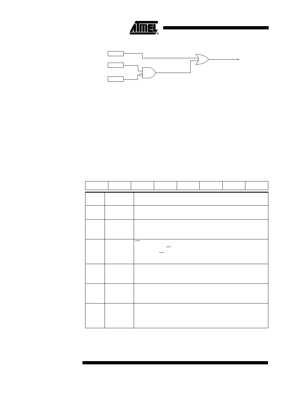
Figure 48. SPI Interrupt Requests Generation
Registers
There are three registers in the module that provide control, status and data storage
functions. These registers are describes in the following paragraphs.
Serial Peripheral Control
Register (SPCON)
•
The Serial Peripheral Control Register does the following:
–
Selects one of the Master clock rates
–
Configure the SPI module as Master or Slave
–
Selects serial clock polarity and phase
–
Enables the SPI module
–
Frees the SS pin for a general-purpose
Table 78 describes this register and explains the use of each bit.
SSDIS
MODF
CPU Interrupt Request
SPI Receiver/Error
CPU Interrupt Request
SPI Transmitter
SPI
CPU Interrupt Request
SPIF
Table 78. SPCON Register
SPCON - Serial Peripheral Control Register (0C3H)
7
6
5
4
3
2
1
0
SPR2
SPEN
SSDIS
MSTR
CPOL
CPHA
SPR1
SPR0
Bit
Number
Bit Mnemonic
Description
7
SPR2
Serial Peripheral Rate 2
Bit with SPR1 and SPR0 define the clock rate.
6
SPEN
Serial Peripheral Enable
Cleared to disable the SPI interface.
Set to enable the SPI interface.
5
SSDIS
SS Disable
Cleared to enable SS in both Master and Slave modes.
Set to disable SS in both Master and Slave modes. In Slave mode, this bit has
no effect if CPHA = “0”.
5
MSTR
Serial Peripheral Master
Cleared to configure the SPI as a Slave.
Set to configure the SPI as a Master.
4
CPOL
Clock Polarity
Cleared to have the SCK set to “0” in idle state.
Set to have the SCK set to “1” in idle low.
3
CPHA
Clock Phase
Cleared to have the data sampled when the SCK leaves the idle state (see
CPOL).
Set to have the data sampled when the SCK returns to idle state (see CPOL).