Flash programming and erasure – Rainbow Electronics AT89C5131 User Manual
Page 54
54
AT89C5131
4136A–USB–03/03
Flash Programming and
Erasure
There are three methods of programming the Flash memory:
•
The Atmel bootloader located in FM1 is activated by the application. Low level API
routines (located in FM1) to program FM0 will be used. The interface used for serial
downloading to FM0 is the UART or the USB. API can be called also by user’s
bootloader located in FM0 at [SBV]00h.
•
A further method exist for activating the Atmel bootloader by using hardware
activation.
•
The FM0 can be also programmed by the parallel mode using a programmer.
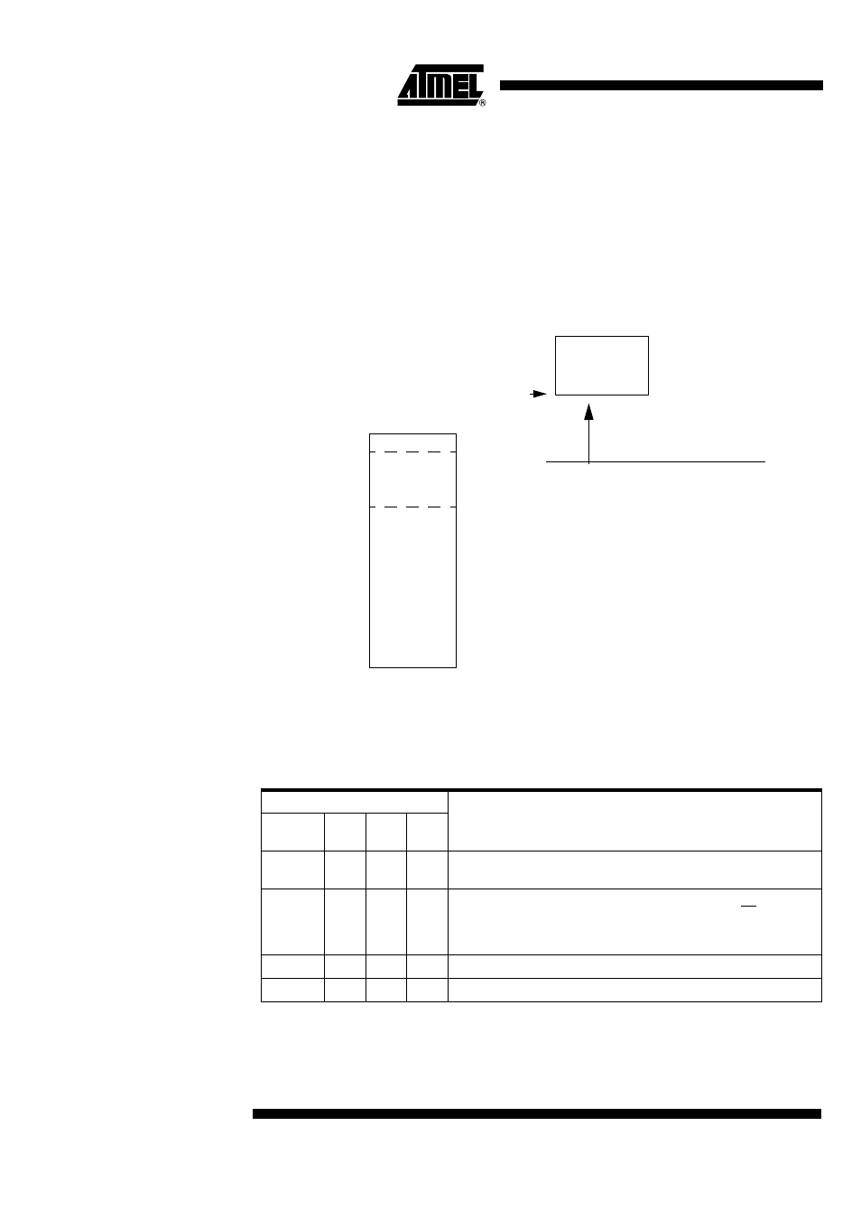
Figure 22. Flash Memory Mapping
Flash Parallel Programming
The three lock bits in Hardware byte are programmed according to Table 43. They will
provide different level of protection for the on-chip code and data located in FM0 and
FM1.
The only way to write these bits are in parallel mode.
Table 43. Program Lock bit
Program Lock bits
U: unprogrammed
P: programmed
F400h
7FFFh
32 Kbytes
Flash Memory
3 Kbytes IAP
Bootloader
FM0
FM1
Custom
Bootloader
[SBV]00h
FFFFh
FM1 mapped between FFFF and F400
when API called
0000h
Program Lock Bits
Protection Description
Security
level
LB0
LB1
LB2
1
U
U
U
No program lock features enabled. MOVC instruction executed from
external program memory returns non encrypted data.
2
P
U
U
MOVC instruction executed from external program memory are
disabled from fetching code bytes from internal memory, EA is sampled
and latched on reset, and further parallel programming of the Flash is
disabled.
3
U
P
U
Same as 2, also verify that parallel programming interface is disabled.
4
U
U
P
Same as 3, also external execution is disabled.