Program/code memory, External code memory access – Rainbow Electronics AT89C5131 User Manual
Page 26
26
AT89C5131
4136A–USB–03/03
Program/Code
Memory
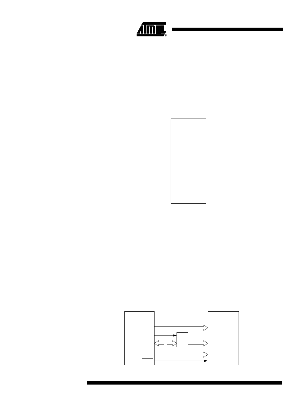
The AT89C5131 implement 32 Kbytes of on-chip program/code memory. Figure 11
shows the split of internal and external program/code memory spaces depending on the
product.
The Flash memory increases EPROM and ROM functionality by in-circuit electrical era-
sure and programming. Thanks to the internal charge pump, the high voltage needed for
programming or erasing Flash cells is generated on-chip using the standard V
DD
volt-
age. Thus, the Flash Memory can be programmed using only one voltage and allows In-
application Software Programming commonly known as IAP. Hardware programming
mode is also available using specific programming tool.
Figure 11. Program/Code Memory Organization
Note:
If the program executes exclusively from on-chip code memory (not from external mem-
ory), beware of executing code from the upper byte of on-chip memory (7FFFh) and
thereby disrupting I/O Ports 0 and 2 due to external prefetch. Fetching code constant
from this location does not affect Ports 0 and 2.
External Code Memory
Access
Memory Interface
The external memory interface comprises the external bus (Port 0 and Port 2) as well as
the bus control signals (PSEN, and ALE).
Figure 12 shows the structure of the external address bus. P0 carries address A7:0
while P2 carries address A15:8. Data D7:0 is multiplexed with A7:0 on P0. Table 31
describes the external memory interface signals.
Figure 12. External Code Memory Interface Structure
0000h
32 Kbytes
7FFFh1
Flash
32 Kbytes
External Code
FFFFh
AT89C5131
8000h
Flash
EPROM
AT89C5131
P2
P0
AD7:0
A15:8
A7:0
A15:8
D7:0
A7:0
ALE
Latch
OE
PSEN